NX3L4053HR,115 NXP Semiconductors, NX3L4053HR,115 Datasheet
NX3L4053HR,115
Specifications of NX3L4053HR,115


Related parts for NX3L4053HR,115


NX3L4053HR,115 Summary of contents
Page 1
NX3L4053 Triple low-ohmic single-pole double-throw analog switch Rev. 3 — 23 December 2010 1. General description The NX3L4053 is a triple low-ohmic single-pole double-throw analog switch, suitable for use as an analog or digital multiplexer/demultiplexer. Each switch has a digital ...
Page 2
... NXP Semiconductors 3. Applications Cell phone PDA Portable media player Analog multiplexing and demultiplexing Digital multiplexing and demultiplexing Signal gating 4. Ordering information Table 1. Ordering information Type number Package Temperature range Name 40 C to +125 C NX3L4053HR NX3L4053PW ...
Page 3
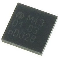
... NXP Semiconductors 6. Functional diagram Pin numbers are shown for TSSOP16 package only. Fig 1. Logic symbol 7. Pinning information 7.1 Pinning terminal 1 index area 3Y1 NX3L4053 3Y0 Transparent top view Fig 3. Pin configuration SOT1039-1 (HXQFN16U) NX3L4053 Product data sheet Triple low-ohmic single-pole double-throw analog switch ...
Page 4
... NXP Semiconductors 7.2 Pin description Table 3. Pin description Symbol Pin SOT1039 n.c. 5 GND 6 1S, 2S 1Y0, 2Y0, 3Y0 10, 16, 3 1Y1, 2Y1, 3Y1 11, 15 2Z, 3Z 12, 13 Functional description Table 4. Function table Inputs [ HIGH voltage level LOW voltage level don’t care. 9. Limiting values Table 5 ...
Page 5
... NXP Semiconductors [2] The minimum and maximum switch voltage ratings may be exceeded if the switch clamping current rating is observed but may not exceed 4.6 V. For HXQFN16U package: above 135 C the value of P [3] For TSSOP16 package: above 60 C the value of P [4] 10. Recommended operating conditions Table 6 ...
Page 6
... NXP Semiconductors Table 7. Static characteristics At recommended operating conditions; voltages are referenced to GND (ground 0 V). Symbol Parameter Conditions I ON-state nZ port; S(ON) leakage current see Figure supply current GND I additional V = GND supply current input nS and I capacitance C OFF-state S(OFF) ...
Page 7
... NXP Semiconductors V IL Fig 6. Test circuit for measuring ON-state leakage current 11.2 ON resistance [1] Table 8. ON resistance At recommended operating conditions; voltages are referenced to GND (ground = 0 V); for graphs see Symbol Parameter Conditions R ON resistance V = GND to V ON(peak) I (peak R ON resistance ...
Page 8
... NXP Semiconductors 11.3 ON resistance test circuit and graphs nY0 switch nZ nY1 2 E GND Fig 7. Test circuit for measuring ON resistance NX3L4053 Product data sheet Triple low-ohmic single-pole double-throw analog switch 1 (Ω) 1.2 0.8 switch 0 001aal741 ( ( ( ( ( ( Measured at T Fig 8. Typical ON resistance as a function of input voltage All information provided in this document is subject to legal disclaimers ...
Page 9
... NXP Semiconductors 1 (Ω) 1.2 0.8 0 125 C. (1) T amb = 85 C. (2) T amb = 25 C. (3) T amb = 40 C. (4) T amb Fig 9. ON resistance as a function of input voltage 1 1 (Ω) 0.8 0.6 0.4 0 125 C. (1) T amb = 85 C. (2) T amb = 25 C. (3) T amb = ...
Page 10
... NXP Semiconductors 1 (Ω) 0.8 0.6 0.4 0 125 C. (1) T amb = 85 C. (2) T amb = 25 C. (3) T amb = 40 C. (4) T amb Fig 13. ON resistance as a function of input voltage 3 12. Dynamic characteristics Table 9. Dynamic characteristics At recommended operating conditions; voltages are referenced to GND (ground = 0 V); for load circuit see ...
Page 11
... NXP Semiconductors Table 9. Dynamic characteristics At recommended operating conditions; voltages are referenced to GND (ground = 0 V); for load circuit see Symbol Parameter Conditions t break-before-make see b-m time [1] Typical values are measured at T [2] Break-before-make guaranteed by design. 12.1 Waveform and test circuits nS, E input output ...
Page 12
... NXP Semiconductors a. Test circuit b. Input and output measurement points Fig 16. Test circuit for measuring break-before-make timing Test data is given in Table Definitions test circuit Load resistance Load capacitance including jig and probe capacitance External voltage for measuring switching times. EXT V may be connected ...
Page 13
... NXP Semiconductors Table 11. Test data Supply voltage 4.3 V 12.2 Additional dynamic characteristics Table 12. Additional dynamic characteristics At recommended operating conditions; voltages are referenced to GND (ground = 0 V); V specified 2.5 ns amb Symbol Parameter THD total harmonic distortion 3 dB frequency f (3dB) response ...
Page 14
... NXP Semiconductors 12.3 Test circuits Fig 18. Test circuit for measuring total harmonic distortion Adjust f voltage to obtain 0 dBm level at output. Increase f i Fig 19. Test circuit for measuring the frequency response when channel is in ON-state V Adjust f voltage to obtain 0 dBm level at input. i Fig 20. Test circuit for measuring isolation (OFF-state) ...
Page 15
... NXP Semiconductors a. Test circuit b. Input and output pulse definitions Fig 21. Test circuit for measuring crosstalk voltage between digital inputs and switch Fig 22. Test circuit for measuring crosstalk between switches NX3L4053 Product data sheet Triple low-ohmic single-pole double-throw analog switch nY0 nY1 ...
Page 16
... NXP Semiconductors a. Test circuit b. Input and output pulse definitions = V C Definition: Q inj O L V = output voltage variation generator resistance. gen V = generator voltage. gen V may be connected Fig 23. Test circuit for measuring charge injection NX3L4053 Product data sheet Triple low-ohmic single-pole double-throw analog switch ...
Page 17
... NXP Semiconductors 13. Package outline HXQFN16U: plastic thermal enhanced extremely thin quad flat package; no leads; 16 terminals; UTLP based; body 0.5 mm terminal 1 index area terminal 1 index area DIMENSIONS (mm are the original dimensions) A UNIT max 0.05 0.35 3.1 mm 0.5 0.00 0.25 2.9 OUTLINE VERSION ...
Page 18
... NXP Semiconductors TSSOP16: plastic thin shrink small outline package; 16 leads; body width 4 pin 1 index 1 DIMENSIONS (mm are the original dimensions) A UNIT max. 0.15 0.95 mm 1.1 0.25 0.05 0.80 Notes 1. Plastic or metal protrusions of 0.15 mm maximum per side are not included. 2. Plastic interlead protrusions of 0.25 mm maximum per side are not included. ...
Page 19
... NXP Semiconductors 14. Abbreviations Table 13. Abbreviations Acronym Description CDM Charged Device Model CMOS Complementary Metal-Oxide Semiconductor ESD ElectroStatic Discharge HBM Human Body Model MM Machine Model PDA Personal Digital Assistant 15. Revision history Table 14. Revision history Document ID Release date NX3L4053 v.3 20101223 • Modifications: Section NX3L4053 v ...
Page 20
... In no event shall NXP Semiconductors be liable for any indirect, incidental, punitive, special or consequential damages (including - without limitation - lost profits, lost savings, business interruption, costs related to the removal or ...
Page 21
... NXP Semiconductors Export control — This document as well as the item(s) described herein may be subject to export control regulations. Export might require a prior authorization from national authorities. 17. Contact information For more information, please visit: For sales office addresses, please send an email to: NX3L4053 Product data sheet Triple low-ohmic single-pole double-throw analog switch 16 ...
Page 22
... NXP Semiconductors 18. Contents 1 General description . . . . . . . . . . . . . . . . . . . . . . 1 2 Features and benefits . . . . . . . . . . . . . . . . . . . . 1 3 Applications . . . . . . . . . . . . . . . . . . . . . . . . . . . . 2 4 Ordering information . . . . . . . . . . . . . . . . . . . . . 2 5 Marking . . . . . . . . . . . . . . . . . . . . . . . . . . . . . . . . 2 6 Functional diagram . . . . . . . . . . . . . . . . . . . . . . 3 7 Pinning information . . . . . . . . . . . . . . . . . . . . . . 3 7.1 Pinning . . . . . . . . . . . . . . . . . . . . . . . . . . . . . . . 3 7.2 Pin description . . . . . . . . . . . . . . . . . . . . . . . . . 4 8 Functional description . . . . . . . . . . . . . . . . . . . 4 9 Limiting values Recommended operating conditions Static characteristics 11.1 Test circuits . . . . . . . . . . . . . . . . . . . . . . . . . . . . 6 11 ...