RDK-249 Power Integrations, RDK-249 Datasheet - Page 22
RDK-249
Manufacturer Part Number
RDK-249
Description
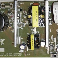
KIT REF DESIGN PFS762HG
Manufacturer
Power Integrations
Series
HiperTFS®r
Specifications of RDK-249
Main Purpose
Reference Design, PC Power Supply
Embedded
No
Utilized Ic / Part
TFS762HG
Primary Attributes
12V 25A, 5V 2.9A Outputs, 300 ~ 385 VDC Input
Output Voltage
5 V
Input / Supply Voltage (max)
385 VDC
Input / Supply Voltage (min)
300 VDC
Duty Cycle (max)
50 %
Mounting Style
Through Hole
Output Current
2.9 A
Output Power
14.5 W
Lead Free Status / RoHS Status
Lead free / RoHS Compliant
Secondary Attributes
-
Other names
596-1398


fSMAX
KI
R(FB)
ILIMIT SELECT
RDS(ON)
DVNOM_GOAL
VDS
Clamp Selection
VCLAMP
VDSOP
DIODE Vf SELECTION
VDMAIN
VDOUT2
VDOUT3
VDB
TRANSFORMER CORE SELECTION
Core Type
Core
Bobbin
AE
LE
AL
BW
M
LG MAX
L
NMAIN
NS2
NBIAS
VOUT2 ACTUAL
VBIAS_ACTUAL
TRANSFORMER DESIGN PARAMETERS
NP
BM_MAX
BM PK-PK
BP_MAX
BP PK-PK
LP MIN
IMAG
OD_P
AWG_P
DUTY CYCLE VALUES (REGULATION)
DVMIN
DVNOM
DVMAX
Power Integrations, Inc.
Tel: +1 408 414 9200 Fax: +1 408 414 9201
www.powerint.com
EER35
150.00
0.448
1.0
CLAMP TO RAIL
EER3
EER35_BOBBIN
5
150.00
570.00
70500
232.0
0.002
20.60
0.123
2770
1791
2714
2321
3516
3.25
3.05
0.45
5.28
1.07
9.08
26.1
3.00
16.3
0.58
0.57
0.45
0.40
1.0
0.5
0.5
0.5
0.7
4.5
7.0
0.0
0.0
88
23
5
mHenries
k-ohms
nH/T^2
Gauss
Gauss
Gauss
Gauss
ohms
cm^2
AWG
P/N:
P/N:
mm
mm
mm
mm
cm
Hz
A
V
V
V
V
V
V
V
V
V
A
Device switching frequency (Maximum)
Select Current limit factor (KI=1.0 for default
ILIMIT, or select KI=0.8 or KI=0.6)
Rds(on) at 100'C
Target duty cycle at nominal input voltage
(VNOM)
HiperTFS average on-state Drain to Source
Voltage
Select either "CLAMP TO RAIL" (default) or
"CLAMP TO GND"
Maximum HiperTFS Drain voltage (at
VOVOFF_MAX)
Main output diodes forward voltage drop
Secondary output diodes forward voltage
drop
3rd output diodes forward voltage drop
Bias diode forward voltage drop
Selected core type
PC40EER35-Z
BEER-35-1116CPH
Core Effective Cross Sectional Area
Core Effective Path Length
Bobbin safety margin tape width (2 * M =
Total Margin)
Maximum zero gap tolerance, default 2um
Transformer primary layers (split primary
recommended)
Main rounded turns
Vout2 rounded secondary turns
(Independent windings)
VBias rounded turns (forward bias winding)
Approximate Output2 voltage of with NS2 = 0
turns (AC stacked secondary)
Approximate Forward Bias Winding Voltage
at VMIN with NB = 5 turns
Primary rounded turns
Max positive operating flux density at
minimum switching frequency
Max peak-peak operating flux density at
minimum switching frequency
Max positive flux density at Vmax (limited by
DVMAX clamp)
Max peak-peak flux density at Vmax (limited
by DVMAX clamp)
Minimum primary magnetizing inductance
(assumes LG MAX=2um)
Peak magnetizing current at minimum input
voltage
Primary wire outer diameter
Primary Wire Gauge (rounded to maximum
AWG value)
Duty cycle at minimum DC input voltage
Duty cycle at nominal DC input voltage
Duty cycle at maximum DC input voltage
Feedback Pin Resistor value
Selected current limit
Asymmetric Clamp Voltage
Ungapped Core Effective Inductance
Bobbin Physical Winding Width
Page 22 of 48
Related parts for RDK-249
Image
Part Number
Description
Manufacturer
Datasheet
Request
R

Part Number:
Description:
KIT REF DESIGN TOP HX FOR TOP258
Manufacturer:
Power Integrations
Datasheet:

Part Number:
Description:
KIT REF DESIGN LINKSWITCH 2
Manufacturer:
Power Integrations
Datasheet:

Part Number:
Description:
KIT REF DESIGN 1.2W PS TN FAMILY
Manufacturer:
Power Integrations
Datasheet:

Part Number:
Description:
KIT REF DESIGN 36-72W MOTOR DRVR
Manufacturer:
Power Integrations
Datasheet:

Part Number:
Description:
KIT REF DESIGN FOR LNK457D
Manufacturer:
Power Integrations
Datasheet:

Part Number:
Description:
REFERENCE DESIGN LINKSWITCH-PH
Manufacturer:
Power Integrations
Datasheet:

Part Number:
Description:
Specifications: Manufacturer: Power Integrations ; Output Voltage: 380 VDC ; Input / Supply Voltage (Max): 264 VAC ; Input / Supply Voltage (Min): 90 VAC ; Mounting Style: Through Hole ; Output Current: 0.913 A ; Output Power: 347 W
Manufacturer:
Power Integrations, Inc.

Part Number:
Description:
Power Management Modules & Development Tools TOPSwitch-JX REF. DESIGN KIT
Manufacturer:
Power Integrations
Datasheet:
Part Number:
Description:
Power Management IC Development Tools REF DESIGN RDR-292 PFF LED STREET LIGHT
Manufacturer:
Power Integrations

Part Number:
Description:
KIT REF DESIGN FOR LNK403EG
Manufacturer:
Power Integrations
Datasheet:

Part Number:
Description:
KIT REF DESIGN FOR LNK406EG
Manufacturer:
Power Integrations
Datasheet:

Part Number:
Description:
KIT REF DESIGN DG CAPZERO
Manufacturer:
Power Integrations
Datasheet:

Part Number:
Description:
KIT REF DESIGN LINKSWITCH-CV
Manufacturer:
Power Integrations
Datasheet:
Part Number:
Description:
Specifications: Family: Eval Boards - DC/DC & AC/DC (Off-Line) SMPS ; Series: HiperLCS™ ; Main Purpose: DC/DC, Step Down ; Outputs and Type: 1, Isolated ; Power - Output: 150W ; Voltage - Output: 24V ; Current - Output: 6.25A ; Voltage - Input:
Manufacturer:
Power Integrations, Inc.
Datasheet:

Part Number:
Description:
KIT REFERENCE DESIGN W/TN376PN
Manufacturer:
Power Integrations
Datasheet: