MNZB-DKC-900 MeshNetics, MNZB-DKC-900 Datasheet - Page 18
MNZB-DKC-900
Manufacturer Part Number
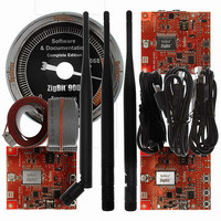
MNZB-DKC-900
Description
KIT DEV ZIGBIT 900 COMPLETE 1YR
Manufacturer
MeshNetics
Type
802.15.4/Zigbeer
Datasheet
1.MNZB-EVB-900-B0.pdf
(56 pages)
Specifications of MNZB-DKC-900
Frequency
868MHz, 915MHz
For Use With/related Products
MNZB-900-B0
Lead Free Status / RoHS Status
Lead free / RoHS Compliant
Other names
758-1009


© 2008 MeshNetics
Pin
17
18
19
20
GENERAL NOTES:
Pins 12, 13, 14, 16, 17, 18 are not buffered and driven by the MCU pins directly. Thus this
interface should be used with precautions at the low supply voltages to avoid damaging
the module.
Pins 7 and 8 are connected via voltage level translators with ESD protection. Thus these
pins can be used easily to connect extra I
Voltage on the V_XX pin does not depend on the state of jumper J1 or ammeter
connection between clamps CM+, CM-.
Table 4. JTAG connector pinout
Pin
1
2
3
4
5
6
7
8
9
10
NOTE:
JTAG connector pinout is compatible with ATmega JTAGICE mkII in-circuit emulator
connector.
Table 5. J1 jumper settings: current measurement
Jumper position
J1 is mounted
Name
ADC_INPUT2
ADC_INPUT3
GND
GND
Name
JTAG_TCK
JTAG_GND
JTAG_TDO
JTAG_VCC
JTAG_TMS
JTAG_RST
N_Cont
N_Cont
JTAG_TDI
JTAG_GND
Z I G B I T ™ 9 0 0 D E V E L O P M E N T K I T 1 . 3
I/O
Input
Input
Description
Scan clock
Digital ground
Test data output
Controller supply voltage
Test mode select
Reset controller; active low
Not connected
Not connected
Test data input
Digital ground
Description
This position is used for normal operation.
2
C sensors without extra logic.
Description
ADC input. This pin is connected directly to the
ADC_INPUT_2 pin of the module. For details,
refer to ZigBit 900 datasheet [1].
ADC input. This pin is connected directly to the
ADC_INPUT_3 pin of the module. For details,
refer to ZigBit 900 datasheet [1].
Digital/analog ground
Digital/analog ground
U S E R ’ S G U I D E
Page 18/56
Related parts for MNZB-DKC-900
Image
Part Number
Description
Manufacturer
Datasheet
Request
R

Part Number:
Description:
KIT DEV ZIGBIT 2.4GHZ COMPLETE
Manufacturer:
MeshNetics
Datasheet:


Part Number:
Description:
MOD 802.15.4/ZIGB 2.4GHZ RF PORT
Manufacturer:
MeshNetics
Datasheet:

Part Number:
Description:
BOARD EVAL FOR MNZB-900-B0 W/ANT
Manufacturer:
MeshNetics
Datasheet:

Part Number:
Description:
BOARD EVAL MNZB-A24-UFL W/RP-SMA
Manufacturer:
MeshNetics


Part Number:
Description:
BOARD DEV 802.15.4/ZIGB PCB ANT
Manufacturer:
MeshNetics
Datasheet:

Part Number:
Description:
BOARD DEV 802.15.4/ZIGB CHIP ANT
Manufacturer:
MeshNetics
Datasheet:

Part Number:
Description:
BOARD DEV 802.15.4/ZIGB SMA CONN
Manufacturer:
MeshNetics
Datasheet:
Part Number:
Description:
KIT DEV ZIGBIT 2.4GHZ LITE 45DAY
Manufacturer:
MeshNetics
Datasheet:

Part Number:
Description:
KIT DEV ZIGBIT 900 LITE 45DAYS
Manufacturer:
MeshNetics
Datasheet:


Part Number:
Description:
MOD 802.15.4/ZIGB 2.4GHZ CHIPANT
Manufacturer:
MeshNetics
Datasheet: