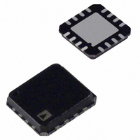
AD8318ACPZ-REEL7 Analog Devices Inc, AD8318ACPZ-REEL7 Datasheet - Page 13

AD8318ACPZ-REEL7
Manufacturer Part Number
AD8318ACPZ-REEL7
Description
IC, LOGARITHMIC AMP, 12NS, LFCSP-16
Manufacturer
Analog Devices Inc
Datasheet
1.AD8318ACPZ-REEL7.pdf
(24 pages)
Specifications of AD8318ACPZ-REEL7
No. Of Amplifiers
1
Dynamic Range, Decades
70
Response Time
12ns
Supply Voltage Range
4.5V To 5.5V
Amplifier Case Style
LFCSP
No. Of Pins
16
Supply Current
68mA
Design Resources
Stable, Closed-Loop Automatic Power Control for RF Appls (CN0050) Software Calibrated, 1 MHz to 8 GHz, 70 dB RF Power Measurement System Using AD8318 (CN0150)
Frequency
1MHz ~ 8GHz
Rf Type
RADAR, 802.11/Wi-Fi, 8.2.16/WiMax, Wireless LAN
Input Range
-60dBm ~ -2dBm
Accuracy
±1dB
Voltage - Supply
4.5 V ~ 5.5 V
Current - Supply
68mA
Package / Case
16-VQFN, CSP Exposed Pad
Rohs Compliant
Yes
Lead Free Status / RoHS Status
Lead free / RoHS Compliant
Other names
AD8318ACPZ-REEL7
AD8318ACPZ-REEL7TR
AD8318ACPZ-REEL7TR
Available stocks
Company
Part Number
Manufacturer
Quantity
Price
Company:
Part Number:
AD8318ACPZ-REEL7
Manufacturer:
FREESCALE
Quantity:
101
While the input can be reactively matched, this is typically not
necessary. An external 52.3 Ω shunt resistor (connected on the
signal side of the input coupling capacitors, see Figure 23)
combines with the relatively high input impedance to provide
an adequate broadband 50 Ω match.
Table 4. Input Impedance for Select Frequency
Frequency
(MHz)
100
450
900
1900
2200
3600
5300
5800
8000
The coupling time constant, 50 × C
corner with a 3 dB attenuation at f
C1 = C2 = C
corner is ~3.2 MHz. In high frequency applications, f
be as large as possible to minimize the coupling of unwanted
low frequency signals. Likewise, in low frequency applications,
a simple RC network forming a low-pass filter should be added,
generally placed at the generator side of the coupling capacitors,
thereby lowering the required capacitance value for a given
high-pass corner frequency.
OUTPUT INTERFACE
The logarithmic output interface is shown in Figure 27. The
VOUT pin is driven by a PNP output stage. An internal 10 Ω
resistor is placed in series with the emitter follower output and
the VOUT pin. The rise time of the output is limited mainly by
the slew on CLPF. The fall time is an RC limited slew provided
by the load capacitance and the pull-down resistance at VOUT.
There is an internal pull-down resistor of 350 Ω. Any resistive
load at VOUT is placed in parallel with the internal pull-down
resistor and provides additional discharge current.
INLO
VPSI
INHI
C
10pF
. Using the typical value of 1 nF, this high-pass
20kΩ
Real
+0.918
+0.905
+0.834
+0.605
+0.524
+0.070
−0.369
−0.326
−0.390
Figure 26. Input Interface
20kΩ
10pF
CURRENT
S11
STAGE
Imaginary
−0.041
−0.183
−0.350
−0.595
−0.616
−0.601
−0.305
−0.286
−0.062
gm
HP
2kΩ
C
/2, forms a high-pass
= 1/(2π × 50 × C
A = 8.6dB
STAGE
FIRST
OFFSET
COMP
GAIN
(Series)
22-j3
Impedance Ω
927-j491
173-j430
61-j233
28-j117
28-j102
26-j49
20-j16
22-j16
HP
C
), where
should
Rev. B | Page 13 of 24
SETPOINT INTERFACE
The setpoint interface is shown in Figure 28. The VSET input
drives the high impedance (250 kΩ) input of an internal
operational amplifier. The VSET voltage appears across the
internal 3.13 kΩ resistor to generate I
of VOUT is applied to VSET, the feedback loop forces
If V
V
The slope is given by −I
example, if a resistor divider to ground is used to generate a
V
−50 mV/dB.
TEMPERATURE COMPENSATION OF OUTPUT
VOLTAGE
The AD8318 functionality includes the capability to externally
trim the temperature drift. Attaching a ground-referenced
resistor to the TADJ pin alters an internal current, minimizing
intercept drift vs. temperature. As a result, the R
optimized for operation at different frequencies.
R
at 2.2 GHz input frequency, is connected between the TADJ pin
and ground (see Figure 23). The value of this resistor partially
determines the magnitude of an analog correction coefficient
that is employed to reduce intercept drift.
TADJ
OUT
SET
SET
−I
voltage of V
, nominally 499 Ω for optimal temperature compensation
= (−I
= V
D
× log
OUT
D
× 3.13 kΩ × X) × log
CMOP
VPSO
CLPF
/X, I
10
(V
OUT
IN
SET
V
INTERNAL
/V
VSET
/2, X = 2. The slope is set to −1 V/decade or
0.2V
= V
Figure 27. Output Interface
+
–
Figure 29. TADJ Interface
INTERCEPT
Figure 28. VSET Interface
2V
D
OUT
× X × 3.13 kΩ = −500 mV × X. For
2kΩ
/(X × 3.13 kΩ). The result is
TADJ
) = I
I
~0.4V
COMP
3.13kΩ
10
SET
(V
CMOP
IN
SET
/V
. When a portion
I
SET
150Ω
200Ω
INTERCEPT
10Ω
VOUT
TADJ
).
AD8318
can be
(2)


