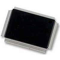
LM97593VH National Semiconductor, LM97593VH Datasheet - Page 27

LM97593VH
Manufacturer Part Number
LM97593VH
Description
12BIT ADC, 2CH, DDC/AGC, 128PQFP
Manufacturer
National Semiconductor
Datasheet
1.LM97593VH.pdf
(50 pages)
Specifications of LM97593VH
Resolution (bits)
12bit
Input Channel Type
Differential
Data Interface
Serial
Supply Voltage Range - Analogue
3V To 3.6V
Supply Voltage Range - Digital
1.6V To 2V, 3V To 3.6V
Supply
RoHS Compliant
Sampling Rate
65MSPS
Rohs Compliant
Yes
Lead Free Status / Rohs Status
Not Compliant
Available stocks
Company
Part Number
Manufacturer
Quantity
Price
Company:
Part Number:
LM97593VH/NOPB
Manufacturer:
VK
Quantity:
1 980
Company:
Part Number:
LM97593VH/NOPB
Manufacturer:
Texas Instruments
Quantity:
10 000
DDC Application Information
3.0 CONTROL INTERFACE
The LM97593 is configured by writing control information into
237 control registers within the chip. The contents of these
control registers and how to use them are described in section
9.1 Control Register Addresses and Defaults. The registers
are written to or read from using the D[7:0], A[7:0], CE, RD
and WR pins. This interface is designed to allow the LM97593
to appear to an external processor as a memory mapped pe-
ripheral. See Figure 15 for details.
The control interface is asynchronous with respect to the sys-
tem clock, CK. This allows the registers to be written or read
at any time. In some cases this might cause an invalid oper-
ation since the interface is not internally synchronized. In
order to assure correct operation, SI must be asserted after
the control registers are written.
The D[7:0], A[7:0], WR, RD and CE pins should not be driven
above the positive supply voltage.
3.1 Master Reset
A master reset pin, MR, is provided to initialize the LM97593
to a known condition and should be strobed after power up.
This signal will clear all sample data and all user programmed
data (filter coefficients and AGC settings). All outputs will be
disabled (tri-stated). ASTROBE and BSTROBE will be as-
serted to initialize the DVGA values. Section 9.1 Control
Register Addresses and Defaults describes the control reg-
ister default values.
3.2 Synchronizing Multiple LM97593 Chips
A system containing two or more LM97593 chips will need to
be synchronized if coherent operation is desired. To synchro-
nize multiple LM97593 chips, connect all of the sync input pins
together so they can be driven by a common sync strobe.
Synchronization occurs on the first rising edge of CK after
SI goes high. When SI is asserted all sample data is imme-
diately cleared, the numerically controlled oscillator (NCO)
phase offset is initialized, the NCO dither generators are re-
set, and the CIC decimation ratio is initialized. Only the con-
figuration data loaded into the microprocessor interface
remains unaffected.
SI may be held low as long as desired after a minimum of 4
CK periods.
FIGURE 19. LM97593 Down Converter, Channel A (Channel B is identical)
27
3.3 Input Source
The input crossbar switch allows either V
register to be routed to the channel A or channel B AGC/ DDC.
The AGC outputs, AGAIN and BGAIN, are not switched. If
V
the AGC will not function properly.
Selecting the test register as the input source allows the AGC
or DDC operation to be verified with a known input. See sec-
tion 8.0 Test and Diagnostics for further discussion.
4.0 DOWN CONVERTERS
A detailed block diagram of each DDC channel is shown in
Figure 19. Each down converter uses a complex NCO and
mixer to quadrature downconvert a signal to baseband. The
“FLOAT TO FIXED CONVERTER” treats the 15-bit mixer
output as a mantissa and the AGC output, EXP, as a 3-bit
exponent. It performs a bit shift on the data based on the value
of EXP. This bit shifting is used to expand the compressed
dynamic range resulting from the DVGA operation. The DV-
GA gain is adjusted in 6dB steps which are equivalent to each
digital bit shift.
Digitally compensating for the DVGA gain steps in the
LM97593 causes the DDC output to be linear with respect to
the DVGA input. The AGC operation will be completely trans-
parent at the LM97593 output.
The exponent (EXP) can be forced to its maximum value by
setting the EXP_INH bit. If x
after the “FLOAT TO FIXED CONVERTER” is
for the I component. Changing the ‘cos’ to ‘sin’ in this equation
will provide the Q component.
The “FLOAT TO FIXED CONVERTER” circuit expands the
dynamic range compression performed by the DVGA. Signals
from this point onward extend across the full dynamic range
of the signals applied to the DVGA input. This allows the AGC
to operate continuously through a burst without producing ar-
tifacts in the signal due to the settling response of the deci-
mation filters after a 6dB DVGA gain adjustment. For
example, if the DVGA input signal were to increase causing
the ADC output level to cross the AGC threshold level, the
gain of the DVGA would change by -6dB. The 6dB step is
allowed to propagate through the ADC and mixers and is
compensated out just before the filtering. The accuracy of
IN
A and V
x
3
IN
(n) = x
B are exchanged the AGC loop will be open and
in
(n)*cos(ωn)*2
in
(n) is the DDC input, the signal
EXP
IN
A, V
(Eq. 5)
IN
www.national.com
B, or a test
30008718


