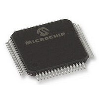
DSPIC30F5011-30I/PTG Microchip Technology, DSPIC30F5011-30I/PTG Datasheet - Page 113

DSPIC30F5011-30I/PTG
Manufacturer Part Number
DSPIC30F5011-30I/PTG
Description
16BIT MCU-DSP 30MHZ, SMD, 30F5011
Manufacturer
Microchip Technology
Series
DsPIC30Fr
Datasheet
1.DSPIC30F5011-30IPTG.pdf
(220 pages)
Specifications of DSPIC30F5011-30I/PTG
Core Frequency
30MHz
Embedded Interface Type
CAN, I2C, SPI, UART
No. Of I/o's
52
Flash Memory Size
66KB
Supply Voltage Range
2.5V To 5.5V
Operating Temperature Range
-40°C To
Lead Free Status / RoHS Status
Lead free / RoHS Compliant
- Current page: 113 of 220
- Download datasheet (4Mb)
17.6.2
There is a programmable prescaler with integral values
ranging from 1 to 64, in addition to a fixed divide-by-2
for clock generation. The time quantum (T
unit of time derived from the oscillator period, and is
given by Equation 17-1, where F
CANCKS bit is set) or 4F
EQUATION 17-1:
17.6.3
This part of the bit time is used to compensate physical
delay times within the network. These delay times con-
sist of the signal propagation time on the bus line and
the internal delay time of the nodes. The Prop Seg can
be programmed from 1 T
PRSEG<2:0> bits (CiCFG2<2:0>).
17.6.4
The phase segments are used to optimally locate the
sampling of the received bit within the transmitted bit
time. The sampling point is between Phase1 Seg and
Phase2 Seg. These segments are lengthened or short-
ened by resynchronization. The end of the Phase1 Seg
determines the sampling point within a bit period. The
segment is programmable from 1 T
Seg provides delay to the next transmitted data transi-
tion. The segment is programmable from 1 T
or it may be defined to be equal to the greater of
Phase1 Seg or the information processing time (2 T
The Phase1 Seg is initialized by setting bits
SEG1PH<2:0> (CiCFG2<5:3>), and Phase2 Seg is
initialized by setting SEG2PH<2:0> (CiCFG2<10:8>).
The following requirement must be fulfilled while setting
the lengths of the phase segments:
2004 Microchip Technology Inc.
Note:
Prop Seg + Phase1 Seg > = Phase2 Seg
PRESCALER SETTING
F
CANCKS = 0, then F
7.5 MHz.
PROPAGATION SEGMENT
PHASE SEGMENTS
T
CAN
Q
= 2 (BRP<5:0> + 1) / F
must not exceed 30 MHz. If
TIME QUANTUM FOR
CLOCK GENERATION
CY
Q
(if CANCKS is clear).
to 8 T
CY
CAN
Q
Q
must not exceed
CAN
to 8 T
by setting the
is F
Q
) is a fixed
Q
CY
Q
. Phase2
to 8 T
(if the
Preliminary
Q
Q
).
,
17.6.5
The sample point is the point of time at which the bus
level is read and interpreted as the value of that respec-
tive bit. The location is at the end of Phase1 Seg. If the
bit timing is slow and contains many T
specify multiple sampling of the bus line at the sample
point. The level determined by the CAN bus then corre-
sponds to the result from the majority decision of three
values. The majority samples are taken at the sample
point and twice before with a distance of T
CAN module allows the user to choose between sam-
pling three times at the same point or once at the same
point, by setting or clearing the SAM bit (CiCFG2<6>).
Typically, the sampling of the bit should take place at
about 60 - 70% through the bit time, depending on the
system parameters.
17.6.6
To compensate for phase shifts between the oscillator
frequencies of the different bus stations, each CAN
controller must be able to synchronize to the relevant
signal edge of the incoming signal. When an edge in
the transmitted data is detected, the logic will compare
the location of the edge to the expected time (Synchro-
nous Segment). The circuit will then adjust the values
of Phase1 Seg and Phase2 Seg. There are 2
mechanisms used to synchronize.
17.6.6.1
Hard synchronization is only done whenever there is a
‘recessive’ to ‘dominant’ edge during bus Idle indicating
the start of a message. After hard synchronization, the
bit time counters are restarted with the Sync Seg. Hard
synchronization forces the edge which has caused the
hard synchronization to lie within the synchronization
segment of the restarted bit time. If a hard synchroniza-
tion is done, there will not be a resynchronization within
that bit time.
17.6.6.2
As a result of resynchronization, Phase1 Seg may be
lengthened or Phase2 Seg may be shortened. The
amount of lengthening or shortening of the phase
buffer segment has an upper bound known as the syn-
chronization jump width, and is specified by the
SJW<1:0> bits (CiCFG1<7:6>). The value of the syn-
chronization jump width will be added to Phase1 Seg or
subtracted from Phase2 Seg. The resynchronization
jump width is programmable between 1 T
The following requirement must be fulfilled while setting
the SJW<1:0> bits:
dsPIC30F5011/5013
Phase2 Seg > Synchronization Jump Width
SAMPLE POINT
SYNCHRONIZATION
Hard Synchronization
Resynchronization
DS70116C-page 111
Q
, it is possible to
Q
and 4 T
Q
/2. The
Q
.
Related parts for DSPIC30F5011-30I/PTG
Image
Part Number
Description
Manufacturer
Datasheet
Request
R

Part Number:
Description:
IC DSPIC MCU/DSP 66K 64TQFP
Manufacturer:
Microchip Technology
Datasheet:

Part Number:
Description:
IC,DSP,16-BIT,CMOS,TQFP,64PIN,PLASTIC
Manufacturer:
Microchip Technology
Datasheet:

Part Number:
Description:
IC DSPIC MCU/DSP 66K 64TQFP
Manufacturer:
Microchip Technology
Datasheet:

Part Number:
Description:
High-Performance Digital Signal Controllers
Manufacturer:
MICROCHIP [Microchip Technology]
Datasheet:

Part Number:
Description:
IC, DSC, 16BIT, 66KB, 40MHZ 5.5V TQFP-64
Manufacturer:
Microchip Technology
Datasheet:

Part Number:
Description:
Digital Signal Processors & Controllers - DSP, DSC 16 Bit MCU/DSP 64LD 20M 66KB FL
Manufacturer:
Microchip Technology

Part Number:
Description:
IC DSPIC MCU/DSP 66K 64TQFP
Manufacturer:
Microchip Technology
Datasheet:

Part Number:
Description:
Dspic30f5011/5013 High-performance Digital Signal Controllers
Manufacturer:
Microchip Technology Inc.
Datasheet:

Part Number:
Description:
Manufacturer:
Microchip Technology Inc.
Datasheet:

Part Number:
Description:
Manufacturer:
Microchip Technology Inc.
Datasheet:

Part Number:
Description:
Manufacturer:
Microchip Technology Inc.
Datasheet:

Part Number:
Description:
Manufacturer:
Microchip Technology Inc.
Datasheet:


