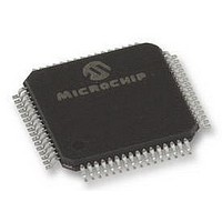
DSPIC30F5011-30I/PTG Microchip Technology, DSPIC30F5011-30I/PTG Datasheet - Page 84

DSPIC30F5011-30I/PTG
Manufacturer Part Number
DSPIC30F5011-30I/PTG
Description
16BIT MCU-DSP 30MHZ, SMD, 30F5011
Manufacturer
Microchip Technology
Series
DsPIC30Fr
Datasheet
1.DSPIC30F5011-30IPTG.pdf
(220 pages)
Specifications of DSPIC30F5011-30I/PTG
Core Frequency
30MHz
Embedded Interface Type
CAN, I2C, SPI, UART
No. Of I/o's
52
Flash Memory Size
66KB
Supply Voltage Range
2.5V To 5.5V
Operating Temperature Range
-40°C To
Lead Free Status / RoHS Status
Lead free / RoHS Compliant
- Current page: 84 of 220
- Download datasheet (4Mb)
dsPIC30F5011/5013
13.1
Each output compare channel can select between one
of two 16-bit timers, Timer2 or Timer3.
The selection of the timers is controlled by the OCTSEL
bit (OCxCON<3>). Timer2 is the default timer resource
for the output compare module.
13.2
When control bits OCM<2:0> (OCxCON<2:0>) = 001,
010 or 011, the selected output compare channel is
configured for one of three simple Output Compare
Match modes:
• Compare forces I/O pin low
• Compare forces I/O pin high
• Compare toggles I/O pin
The OCxR register is used in these modes. The OCxR
register is loaded with a value and is compared to the
selected incrementing timer count. When a compare
occurs, one of these Compare Match modes occurs. If
the counter resets to zero before reaching the value in
OCxR, the state of the OCx pin remains unchanged.
13.3
When control bits OCM<2:0> (OCxCON<2:0>) = 100
or 101, the selected output compare channel is config-
ured for one of two Dual Output Compare modes,
which are:
• Single Output Pulse mode
• Continuous Output Pulse mode
13.3.1
For the user to configure the module for the generation
of a single output pulse, the following steps are
required (assuming timer is off):
• Determine instruction cycle time T
• Calculate desired pulse width value based on T
• Calculate time to start pulse from timer start value
• Write pulse width start and stop times into OCxR
• Set Timer Period register to value equal to, or
• Set OCM<2:0> = 100.
• Enable timer, TON (TxCON<15>) = 1.
To initiate another single pulse, issue another write to
set OCM<2:0> = 100.
DS70116C-page 82
of 0x0000.
and OCxRS Compare registers (x denotes
channel 1, 2, ...,N).
greater than value in OCxRS Compare register.
Timer2 and Timer3 Selection Mode
Simple Output Compare Match
Mode
Dual Output Compare Match Mode
SINGLE PULSE MODE
CY
.
CY
Preliminary
.
13.3.2
For the user to configure the module for the generation
of a continuous stream of output pulses, the following
steps are required:
• Determine instruction cycle time T
• Calculate desired pulse value based on T
• Calculate timer to start pulse width from timer start
• Write pulse width start and stop times into OCxR
• Set Timer Period register to value equal to, or
• Set OCM<2:0> = 101.
• Enable timer, TON (TxCON<15>) = 1.
13.4
When control bits OCM<2:0> (OCxCON<2:0>) = 110
or 111, the selected output compare channel is config-
ured for the PWM mode of operation. When configured
for the PWM mode of operation, OCxR is the main latch
(read only) and OCxRS is the secondary latch. This
enables glitchless PWM transitions.
The user must perform the following steps in order to
configure the output compare module for PWM
operation:
1.
2.
3.
4.
13.4.1
When control bits OCM<2:0> (OCxCON<2:0>) = 111,
the selected output compare channel is again config-
ured for the PWM mode of operation with the additional
feature of input FAULT protection. While in this mode,
if a logic ‘0’ is detected on the OCFA/B pin, the respec-
tive PWM output pin is placed in the high impedance
input state. The OCFLT bit (OCxCON<4>) indicates
whether a FAULT condition has occurred. This state will
be maintained until both of the following events have
occurred:
• The external FAULT condition has been removed.
• The PWM mode has been re-enabled by writing
value of 0x0000.
and OCxRS (x denotes channel 1, 2, ...,N)
Compare registers, respectively.
greater than value in OCxRS Compare register.
to the appropriate control bits.
Set the PWM period by writing to the appropriate
period register.
Set the PWM duty cycle by writing to the OCxRS
register.
Configure the output compare module for PWM
operation.
Set the TMRx prescale value and enable the
Timer, TON (TxCON<15>) = 1.
Simple PWM Mode
CONTINUOUS PULSE MODE
INPUT PIN FAULT PROTECTION
FOR PWM
2004 Microchip Technology Inc.
CY
.
CY
.
Related parts for DSPIC30F5011-30I/PTG
Image
Part Number
Description
Manufacturer
Datasheet
Request
R

Part Number:
Description:
IC DSPIC MCU/DSP 66K 64TQFP
Manufacturer:
Microchip Technology
Datasheet:

Part Number:
Description:
IC,DSP,16-BIT,CMOS,TQFP,64PIN,PLASTIC
Manufacturer:
Microchip Technology
Datasheet:

Part Number:
Description:
IC DSPIC MCU/DSP 66K 64TQFP
Manufacturer:
Microchip Technology
Datasheet:

Part Number:
Description:
High-Performance Digital Signal Controllers
Manufacturer:
MICROCHIP [Microchip Technology]
Datasheet:

Part Number:
Description:
IC, DSC, 16BIT, 66KB, 40MHZ 5.5V TQFP-64
Manufacturer:
Microchip Technology
Datasheet:

Part Number:
Description:
Digital Signal Processors & Controllers - DSP, DSC 16 Bit MCU/DSP 64LD 20M 66KB FL
Manufacturer:
Microchip Technology

Part Number:
Description:
IC DSPIC MCU/DSP 66K 64TQFP
Manufacturer:
Microchip Technology
Datasheet:

Part Number:
Description:
Dspic30f5011/5013 High-performance Digital Signal Controllers
Manufacturer:
Microchip Technology Inc.
Datasheet:

Part Number:
Description:
Manufacturer:
Microchip Technology Inc.
Datasheet:

Part Number:
Description:
Manufacturer:
Microchip Technology Inc.
Datasheet:

Part Number:
Description:
Manufacturer:
Microchip Technology Inc.
Datasheet:

Part Number:
Description:
Manufacturer:
Microchip Technology Inc.
Datasheet:


