ADSP-TS201SABPZ060 Analog Devices Inc, ADSP-TS201SABPZ060 Datasheet - Page 12
ADSP-TS201SABPZ060
Manufacturer Part Number
ADSP-TS201SABPZ060
Description
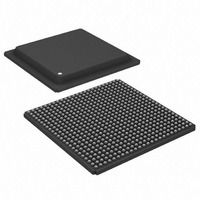
IC, FLOAT-PT DSP, 64BIT, 600MHZ, BGA-576
Manufacturer
Analog Devices Inc
Series
TigerSHARCr
Type
Fixed/Floating Pointr
Datasheet
1.ADSP-TS201SABPZ050.pdf
(48 pages)
Specifications of ADSP-TS201SABPZ060
Frequency
600MHz
Supply Voltage
1.2V
Embedded Interface Type
HPI
No. Of I/o's
4
Supply Voltage Range
1.14V To 1.26V, 2.38V To 2.63V
Interface
Host Interface, Link Port, Multi-Processor
Clock Rate
600MHz
Non-volatile Memory
External
On-chip Ram
3MB
Voltage - I/o
2.50V
Voltage - Core
1.20V
Operating Temperature
-40°C ~ 85°C
Mounting Type
Surface Mount
Package / Case
576-BGA
Lead Free Status / RoHS Status
Lead free / RoHS Compliant
For Use With
ADZS-TS201S-EZLITE - KIT LITE EVAL FOR ADSP-TS201S
Lead Free Status / RoHS Status
Lead free / RoHS Compliant, Lead free / RoHS Compliant
Available stocks
Company
Part Number
Manufacturer
Quantity
Price
Company:

Part Number:
ADSP-TS201SABPZ060
Manufacturer:
MOLEX
Quantity:
12 000
Company:
Part Number:
ADSP-TS201SABPZ060
Manufacturer:
ADI42
Quantity:
693
Company:
Part Number:
ADSP-TS201SABPZ060
Manufacturer:
Analog Devices Inc
Quantity:
10 000


ADSP-TS201S
PIN FUNCTION DESCRIPTIONS
While most of the ADSP-TS201S processor’s input pins are nor-
mally synchronous—tied to a specific clock—a few are
asynchronous. For these asynchronous signals, an on-chip syn-
chronization circuit prevents metastability problems. Use the ac
specification for asynchronous signals when the system design
requires predictable, cycle-by-cycle behavior for these signals.
Table 3. Pin Definitions—Clocks and Reset
Table 4. SCLK Ratio
Signal
SCLKRAT2–0
SCLK
RST_IN
RST_OUT
POR_IN
I = input; A = asynchronous; O = output; OD = open-drain output; T = three-state; P = power supply; G = ground; pd = internal pull-down
5 k
pull-up 500
= internal pull-up 40 k
Term (termination of unused pins) column symbols: epd = external pull-down approximately 5 k
imately 5 k
SCLKRAT2–0
000
001
010
011
100
101
110
111
Ω
; pu = internal pull-up 5 k
(default)
Ω
Ω
to V
on DSP ID = 0; pd_m = internal pull-down 5 k
DD_IO
, nc = not connected; na = not applicable (always used); V
Ω
. For more pull-down and pull-up information, see
I (pd)
Type
I
I/A
O
I/A
Ω
; pd_0 = internal pull-down 5 k
Ratio
4
5
6
7
8
10
12
Reserved
Term
na
na
na
na
na
Rev. C | Page 12 of 48 | December 2006
Description
Core Clock Ratio. The DSP’s core clock (CCLK) rate = n × SCLK, where n is user-
programmable using the SCLKRATx pins to the values shown in
may change only during reset; connect these pins to V
tions in
is the instruction cycle rate.
System Clock Input. The DSP’s system input clock for cluster bus. The core clock rate
is user-programmable using the SCLKRATx pins.
Domains on Page 9.
Reset. Sets the DSP to a known state and causes program to be in idle state. RST_IN
must be asserted a specified time according to the type of reset operation. For details,
see
Reset Output. Indicates that the DSP reset is complete. Connect to POR_IN.
Power-On Reset for internal DRAM. Connect to RST_OUT.
Reset and Booting on Page
Ω
Ω
on DSP bus master; pu_m = internal pull-up 5 k
on DSP ID = 0; pu_0 = internal pull-up 5 k
Table
25,
Table
The output pins can be three-stated during normal operation.
The DSP three-states all output pins during reset, allowing these
pins to get to their internal pull-up or pull-down state. Some
pins have an internal pull-up or pull-down resistor (±30% toler-
ance) that maintains a known value during transitions between
different drivers.
Electrical Characteristics on Page
26, and
DD_IO
= connect directly to V
Table 27
9,
Table 25 on Page
must be satisfied. The core clock rate (CCLK)
Ω
to V
Ω
For more information, see Clock
on DSP ID = 0; pu_od_0 = internal
SS
DD_IO
26, and
; epu = external pull-up approx-
22.
DD_IO
Ω
; V
on DSP bus master; pu_ad
SS
or V
Figure 13 on Page
= connect directly to V
SS
Table
. All reset specifica-
4. These pins
26.
SS
Related parts for ADSP-TS201SABPZ060
Image
Part Number
Description
Manufacturer
Datasheet
Request
R

Part Number:
Description:
±1.7g Dual-Axis IMEMS Accelerometer Evaluation Board
Manufacturer:
Analog Devices Inc
Datasheet:

Part Number:
Description:
Inertial Sensor Evaluation System
Manufacturer:
Analog Devices Inc
Datasheet:
Part Number:
Description:
Manufacturer:
Analog Devices Inc
Datasheet:
Part Number:
Description:
Manufacturer:
Analog Devices Inc
Datasheet:
Part Number:
Description:
Manufacturer:
Analog Devices Inc
Datasheet:
Part Number:
Description:
Manufacturer:
Analog Devices Inc
Datasheet:
Part Number:
Description:
Manufacturer:
Analog Devices Inc
Datasheet:
Part Number:
Description:
Manufacturer:
Analog Devices Inc
Datasheet:
Part Number:
Description:
Manufacturer:
Analog Devices Inc
Datasheet:
Part Number:
Description:
Manufacturer:
Analog Devices Inc
Datasheet:
Part Number:
Description:
Manufacturer:
Analog Devices Inc
Datasheet:
Part Number:
Description:
Manufacturer:
Analog Devices Inc
Datasheet:
Part Number:
Description:
Manufacturer:
Analog Devices Inc
Datasheet: