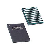
EPM7256AEFC256-10N Altera, EPM7256AEFC256-10N Datasheet - Page 54

EPM7256AEFC256-10N
Manufacturer Part Number
EPM7256AEFC256-10N
Description
IC PLD EEPROM 256 MACROCELL FBGA-256
Manufacturer
Altera
Series
MAX 7000AEr
Datasheet
1.EPM7032AELC44-10N.pdf
(64 pages)
Specifications of EPM7256AEFC256-10N
Cpld Type
EEPROM
No. Of Macrocells
256
No. Of I/o's
164
Propagation Delay
10ns
Global Clock Setup Time
3.9ns
Frequency
172.4MHz
Supply Voltage Range
3V To 3.6V
Family Name
MAX 7000A
Memory Type
EEPROM
# Macrocells
256
Number Of Usable Gates
5000
Frequency (max)
125MHz
Propagation Delay Time
10ns
Number Of Logic Blocks/elements
16
# I/os (max)
164
Operating Supply Voltage (typ)
3.3V
In System Programmable
Yes
Operating Supply Voltage (min)
3V
Operating Supply Voltage (max)
3.6V
Operating Temp Range
0C to 70C
Operating Temperature Classification
Commercial
Mounting
Surface Mount
Pin Count
256
Package Type
FBGA
Rohs Compliant
Yes
Lead Free Status / RoHS Status
Lead free / RoHS Compliant
Lead Free Status / RoHS Status
Lead free / RoHS Compliant
Available stocks
Company
Part Number
Manufacturer
Quantity
Price
Part Number:
EPM7256AEFC256-10N
Manufacturer:
ALTERA/阿尔特拉
Quantity:
20 000
MAX 7000A Programmable Logic Device Data Sheet
Notes to tables:
(1)
(2)
(3)
(4)
(5)
(6)
Power
Consumption
54
t
t
t
t
t
t
t
t
Symbol
COMB
IC
EN
GLOB
PRE
CLR
PIA
LPA
Table 30. EPM7256A Internal Timing Parameters (Part 2 of 2)
These values are specified under the recommended operating conditions shown in
Figure 12
These values are specified for a PIA fan-out of one LAB (16 macrocells). For each additional LAB fan-out in these
devices, add an additional 0.1 ns to the PIA timing value.
This minimum pulse width for preset and clear applies for both global clear and array controls. The t
must be added to this minimum width if the clear or reset signal incorporates the t
path.
This parameter is measured with a 16-bit loadable, enabled, up/down counter programmed into each LAB.
Operating conditions: V
The t
running in low-power mode.
LPA
Combinatorial delay
Array clock delay
Register enable time
Global control delay
Register preset time
Register clear time
PIA delay
Low-power adder
parameter must be added to the t
for more information on switching waveforms.
Parameter
CCIO
Supply power (P) versus frequency (f
devices is calculated with the following equation:
P = P
The P
and switching frequency, can be calculated using the guidelines given in
Application Note 74 (Evaluating Power for Altera Devices).
The I
logic. The I
I
(A × MC
CCINT
= 2.5 ± 0.2 V for commercial and industrial use.
CCINT
INT
IO
(2)
(6)
Conditions
=
value, which depends on the device output load characteristics
TON
+ P
CCINT
value depends on the switching frequency and the application
IO
) + [B × (MC
LAD
= I
, t
value is calculated with the following equation:
CCINT
LAC
Min
, t
IC
-6
, t
× V
DEV
Max
11.0
EN
1.6
2.7
2.5
1.1
2.3
2.3
1.3
CC
, t
SEXP
– MC
+ P
Min
, t
IO
ACL
TON
-7
Note (1)
Speed Grade
Max
10.0
MAX
, and t
2.0
3.4
3.1
1.4
2.9
2.9
1.6
)] + (C × MC
, in MHz) for MAX 7000A
CPPW
Min
LAD
Table 14 on page
-10
parameters for macrocells
Max
10.0
parameter into the signal
2.7
4.5
4.2
1.8
3.8
3.8
2.1
USED
Altera Corporation
Min
× f
MAX
-12
LPA
28. See
Max
10.0
3.2
5.4
5.0
2.2
4.6
4.6
2.6
parameter
× tog
Unit
ns
ns
ns
ns
ns
ns
ns
ns
LC
)


