74HC21D NXP Semiconductors, 74HC21D Datasheet
74HC21D
Specifications of 74HC21D
Available stocks


Related parts for 74HC21D


74HC21D Summary of contents
Page 1
Dual 4-input AND gate Rev. 03 — 12 November 2004 1. General description The 74HC21 is a high-speed Si-gate CMOS device and is pin compatible with low-power Schottky TTL (LSTTL). The 74HC21 is specified in compliance with JEDEC standard ...
Page 2
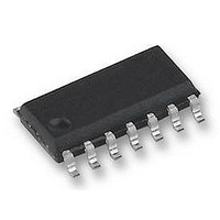
... Ordering information Table 2: Ordering information Type number Package Temperature range Name 74HC21N +125 C 74HC21D +125 C 74HC21DB +125 C 5. Functional diagram Fig 1. Functional diagram Fig 3. IEC logic symbol 9397 750 13806 Product data sheet Description DIP14 plastic dual in-line package; 14 leads (300 mil) SO14 plastic small outline package ...
Page 3
Philips Semiconductors 6. Pinning information 6.1 Pinning Fig 5. Pin configuration 6.2 Pin description Table 3: Symbol GND n. 9397 750 13806 Product data sheet 1A 1 ...
Page 4
Philips Semiconductors 7. Functional description 7.1 Function table Table 4: Input [ HIGH voltage level LOW voltage level don’t care. 8. Limiting values Table 5: In accordance with ...
Page 5
Philips Semiconductors 9. Recommended operating conditions Table 6: Symbol amb 10. Static characteristics Table 7: Static characteristics At recommended operating conditions; voltages are referenced to GND (ground = ...
Page 6
Philips Semiconductors Table 7: Static characteristics At recommended operating conditions; voltages are referenced to GND (ground = 0 V). Symbol Parameter +85 C amb V HIGH-level input voltage IH V LOW-level input voltage IL V ...
Page 7
Philips Semiconductors Table 7: Static characteristics At recommended operating conditions; voltages are referenced to GND (ground = 0 V). Symbol Parameter +125 C amb V HIGH-level input voltage IH V LOW-level input voltage IL V ...
Page 8
Philips Semiconductors 11. Dynamic characteristics Table 8: Dynamic characteristics GND = ns pF; see Symbol Parameter amb propagation delay nA, ...
Page 9
Philips Semiconductors 12. Waveforms Fig 6. Waveforms showing the input (nA, nB, nC, nD) to output (nY) propagation delays Fig 7. Load circuitry for switching times Table 9: Supply V CC 2.0 V 4.5 V 6.0 V 5.0 V 9397 ...
Page 10
Philips Semiconductors 13. Package outline DIP14: plastic dual in-line package; 14 leads (300 mil pin 1 index 1 DIMENSIONS (inch dimensions are derived from the original mm dimensions UNIT max. min. max. ...
Page 11
Philips Semiconductors SO14: plastic small outline package; 14 leads; body width 3 pin 1 index 1 e DIMENSIONS (inch dimensions are derived from the original mm dimensions) A UNIT max. ...
Page 12
Philips Semiconductors SSOP14: plastic shrink small outline package; 14 leads; body width 5 pin 1 index 1 e DIMENSIONS (mm are the original dimensions) A UNIT max. 0.21 1.80 mm ...
Page 13
Philips Semiconductors 14. Revision history Table 10: Revision history Document ID Release date 74HC21_3 20041112 • Modifications: The format of this data sheet has been redesigned to comply with the current presentation and information standard of Philips Semiconductors. • Removed ...
Page 14
Philips Semiconductors 15. Data sheet status [1] Level Data sheet status Product status I Objective data Development II Preliminary data Qualification III Product data Production [1] Please consult the most recently issued data sheet before initiating or completing a design. ...
Page 15
Philips Semiconductors 19. Contents 1 General description . . . . . . . . . . . . . . . . . . . . . . 1 2 Features . . . . . . . . ...