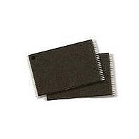
S29JL032H90TFI320 Spansion Inc., S29JL032H90TFI320 Datasheet - Page 28

S29JL032H90TFI320
Manufacturer Part Number
S29JL032H90TFI320
Description
IC, FLASH, 32MBIT, 90NS, TSOP-48
Manufacturer
Spansion Inc.
Datasheet
1.S29JL032H90TFI320.pdf
(61 pages)
Specifications of S29JL032H90TFI320
Memory Type
Flash
Memory Size
32Mbit
Memory Configuration
4M X 8 / 2M X 16
Ic Interface Type
CFI, Parallel
Access Time
90ns
Supply Voltage Range
2.7 To 3.6 V
Memory Case Style
TSOP
Data Bus Width
8 bit, 16 bit
Architecture
Boot Sector
Interface Type
Conventional
Supply Voltage (max)
3.6 V
Supply Voltage (min)
2.7 V
Maximum Operating Current
2 mA
Mounting Style
SMD/SMT
Operating Temperature
+ 85 C
Package / Case
TSOP-48
Rohs Compliant
YES
No. Of Pins
48
Lead Free Status / RoHS Status
Lead free / RoHS Compliant
Lead Free Status / RoHS Status
Lead free / RoHS Compliant, Lead free / RoHS Compliant
Available stocks
Company
Part Number
Manufacturer
Quantity
Price
Company:
Part Number:
S29JL032H90TFI320
Manufacturer:
Spansion
Quantity:
135
Company:
Part Number:
S29JL032H90TFI320
Manufacturer:
PANASONIC
Quantity:
4 314
Part Number:
S29JL032H90TFI320
Manufacturer:
SPANSION
Quantity:
20 000
9. Common Flash Memory Interface (CFI)
28
The Common Flash Interface (CFI) specification outlines device and host system software interrogation
handshake, which allows specific vendor-specified software algorithms to be used for entire families of
devices. Software support can then be device-independent, JEDEC ID-independent, and forward- and
backward-compatible for the specified flash device families. Flash vendors can standardize their existing
interfaces for long-term compatibility.
This device enters the CFI Query mode when the system writes the CFI Query command, 98h, to address
55h in word mode (or address AAh in byte mode), any time the device is ready to read array data. The system
can read CFI information at the addresses given in
must write the reset command. The CFI Query mode is not accessible when the device is executing an
Embedded Program or embedded Erase algorithm.
The system can also write the CFI query command when the device is in the autoselect mode. The device
enters the CFI query mode, and the system can read CFI data at the addresses given in
system must write the reset command to reading array data.
For further information, please refer to the CFI Specification and CFI Publication 100. Contact your local sales
office for copies of these documents.
(Word Mode)
(Word Mode)
Addresses
Addresses
1Bh
1Ch
1Dh
1Eh
1Fh
20h
21h
22h
23h
24h
25h
26h
1Ah
10h
11h
12h
13h
14h
15h
16h
17h
18h
19h
(Byte Mode)
Addresses
(Byte Mode)
Addresses
3Ch
4Ch
36h
38h
3Ah
3Eh
40h
42h
44h
46h
48h
4Ah
2Ah
2Ch
2Eh
20h
22h
24h
26h
28h
30h
32h
34h
0027h
0036h
0000h
0000h
0003h
0000h
0009h
0000h
0005h
0000h
0004h
0000h
Data
Table 9.1 CFI Query Identification String
0051h
0052h
0059h
0002h
0000h
0040h
0000h
0000h
0000h
0000h
0000h
Data
Table 9.2 System Interface String
S29JL032H
V
D7–D4: volt, D3–D0: 100 millivolt
V
D7–D4: volt, D3–D0: 100 millivolt
V
V
Typical timeout per single byte/word write 2
Typical timeout for Min. size buffer write 2
Typical timeout per individual block erase 2
Typical timeout for full chip erase 2
Max. timeout for byte/word write 2
Max. timeout for buffer write 2
Max. timeout per individual block erase 2
Max. timeout for full chip erase 2
CC
CC
PP
PP
D a t a
Min. voltage (00h = no V
Max. voltage (00h = no V
Min. (write/erase)
Max. (write/erase)
Query Unique ASCII string “QRY”
Primary OEM Command Set
Address for Primary Extended Table
Alternate OEM Command Set (00h = none exists)
Address for Alternate OEM Extended Table (00h = none exists)
Table
S h e e t
9.1. To terminate reading CFI data, the system
PP
PP
N
times typical
pin present)
N
pin present)
N
times typical (00h = not supported)
N
times typical
Description
ms (00h = not supported)
Description
S29JL032H_00_B8 August 31, 2009
N
N
times typical
µ
N
N
ms
µs
s (00h = not supported)
Table
9.1. The


