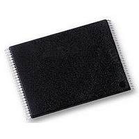
AM29F160DB-90EF Spansion Inc., AM29F160DB-90EF Datasheet - Page 22

AM29F160DB-90EF
Manufacturer Part Number
AM29F160DB-90EF
Description
IC, FLASH, 16MBIT, 90NS, TSOP-48
Manufacturer
Spansion Inc.
Datasheet
1.AM29F160DB-70EF.pdf
(47 pages)
Specifications of AM29F160DB-90EF
Memory Type
Flash
Memory Size
16Mbit
Memory Configuration
2M X 8 / 1M X 16
Ic Interface Type
Parallel
Access Time
90ns
Supply Voltage Range
4.5V To 5.5V
Memory Case Style
TSOP
No. Of Pins
48
Lead Free Status / RoHS Status
Lead free / RoHS Compliant
Available stocks
Company
Part Number
Manufacturer
Quantity
Price
Company:
Part Number:
AM29F160DB-90EF
Manufacturer:
FREESCALE
Quantity:
101
Note: See the appropriate Command Definitions table for
program command sequence.
Chip Erase Command Sequence
Chip erase is a six-bus-cycle operation. The chip erase
command sequence is initiated by writing two unlock
cycles, followed by a set-up command. Two additional
unlock write cycles are then followed by the chip erase
command, which in turn invokes the Embedded Erase
algorithm. The device does not require the system to
preprogram prior to erase. The Embedded Erase algo-
rithm automatically preprograms and verifies the entire
memory for an all zero data pattern prior to electrical
erase. The system is not required to provide any con-
trols or timings during these operations. The Command
Definitions table shows the address and data require-
ments for the chip erase command sequence.
Any commands written to the chip during the Embed-
ded Erase algorithm are ignored. Note that a hardware
reset during the chip erase operation immediately ter-
minates the operation. The Chip Erase command se-
quence should be reinitiated once the device returns to
reading array data, to ensure data integrity.
20
Increment Address
Figure 3. Program Operation
in progress
Embedded
algorithm
Program
No
Command Sequence
Write Program
Last Address?
Programming
from System
Verify Data?
Completed
Data Poll
START
Yes
Yes
D A T A S H E E T
No
Am29F160D
The system can determine the status of the erase
operation by using DQ7, DQ6, DQ2, or RY/BY#. See
on these status bits. When the Embedded Erase al-
gorithm is complete, the device returns to reading
array data and addresses are no longer latched.
Figure 4, on page 21
erase operation. See the Erase/Program Operations
tables in “AC Characteristics” for parameters, and to
the Chip/Sector Erase Operation Timings for timing
waveforms.
Sector Erase Command Sequence
Sector erase is a six bus cycle operation. The sector
erase command sequence is initiated by writing two un-
lock cycles, followed by a set-up command. Two addi-
tional unlock write cycles are then followed by the
address of the sector to be erased, and the sector
erase command. The Command Definitions table
shows the address and data requirements for the sec-
tor erase command sequence.
The device does not require the system to preprogram
the memory prior to erase. The Embedded Erase algo-
rithm automatically programs and verifies the sector for
an all zero data pattern prior to electrical erase. The
system is not required to provide any controls or tim-
ings during these operations.
After the command sequence is written, a sector erase
time-out of 50 µs begins. During the time-out period,
additional sector addresses and sector erase com-
mands may be written. Loading the sector erase buffer
may be done in any sequence, and the number of sec-
tors may be from one sector to all sectors. The time be-
tween these additional cycles must be less than 50 µs,
otherwise the last address and command might not be
accepted, and erasure may begin. It is recommended
that processor interrupts be disabled during this time to
ensure all commands are accepted. The interrupts can
be re-enabled after the last Sector Erase command is
written. If the time between additional sector erase
commands can be assumed to be less than 50 µs, the
system need not monitor DQ3. Any command other
than Sector Erase or Erase Suspend during the
time-out period resets the device to reading array
data. The system must rewrite the command sequence
and any additional sector addresses and commands.
The system can monitor DQ3 to determine if the sector
erase timer has timed out. (See the
Timer‚ on page 25
the rising edge of the final WE# pulse in the command
sequence.
Once the sector erase operation begins, only the Erase
Suspend command is valid. All other commands are ig-
nored. Note that a hardware reset during the sector
erase operation immediately terminates the operation.
Write Operation Status‚ on page 23
section.) The time-out begins from
illustrates the algorithm for the
Am29F160D_00_D10 April 23, 2010
DQ3: Sector Erase
for information


