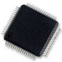
LPC2132FBD64 NXP Semiconductors, LPC2132FBD64 Datasheet - Page 12

LPC2132FBD64
Manufacturer Part Number
LPC2132FBD64
Description
16/32BIT MCU ARM7, 64K FLASH, 64LQFP
Manufacturer
NXP Semiconductors
Datasheet
1.LPC2131FBD64.pdf
(45 pages)
Specifications of LPC2132FBD64
No. Of I/o's
47
Ram Memory Size
16KB
Cpu Speed
60MHz
No. Of Timers
2
No. Of Pwm Channels
6
Digital Ic Case
RoHS Compliant
Core Size
32bit
Program Memory Size
64KB
Oscillator Type
External Only
Controller Family/series
LPC21xx
Rohs Compliant
Yes
Available stocks
Company
Part Number
Manufacturer
Quantity
Price
Company:
Part Number:
LPC2132FBD64
Manufacturer:
PHILIPS
Quantity:
5
Part Number:
LPC2132FBD64
Manufacturer:
NXP/恩智浦
Quantity:
20 000
Company:
Part Number:
LPC2132FBD64,151
Manufacturer:
NXP Semiconductors
Quantity:
10 000
Company:
Part Number:
LPC2132FBD64/01
Manufacturer:
NXP
Quantity:
5 530
Company:
Part Number:
LPC2132FBD64/01
Manufacturer:
NXP
Quantity:
2 844
Company:
Part Number:
LPC2132FBD64/01
Manufacturer:
NXP
Quantity:
8 000
Part Number:
LPC2132FBD64/01
Manufacturer:
NXP/恩智浦
Quantity:
20 000
Company:
Part Number:
LPC2132FBD64/01,11
Manufacturer:
NXP Semiconductors
Quantity:
10 000
Company:
Part Number:
LPC2132FBD64/01,15
Manufacturer:
NXP Semiconductors
Quantity:
10 000
Part Number:
LPC2132FBD64/01.151
Manufacturer:
NXP/恩智浦
Quantity:
20 000
NXP Semiconductors
Table 3.
[1]
[2]
[3]
[4]
[5]
[6]
[7]
[8]
[9]
LPC2131_32_34_36_38
Product data sheet
Symbol
P1.26/RTCK
P1.27/TDO
P1.28/TDI
P1.29/TCK
P1.30/TMS
P1.31/TRST
RESET
XTAL1
XTAL2
RTCX1
RTCX2
V
V
V
V
VREF
VBAT
SS
SSA
DD
DDA
5 V tolerant pad providing digital I/O functions with TTL levels and hysteresis and 10 ns slew rate control.
5 V tolerant pad providing digital I/O functions with TTL levels and hysteresis and 10 ns slew rate control. If configured for an input
function, this pad utilizes built-in glitch filter that blocks pulses shorter than 3 ns.
Open drain 5 V tolerant digital I/O I
functionality.
5 V tolerant pad providing digital I/O (with TTL levels and hysteresis and 10 ns slew rate control) and analog input function. If configured
for an input function, this pad utilizes built-in glitch filter that blocks pulses shorter than 3 ns. When configured as an ADC input, digital
section of the pad is disabled.
5 V tolerant pad providing digital I/O (with TTL levels and hysteresis and 10 ns slew rate control) and analog output function. When
configured as the DAC output, digital section of the pad is disabled.
5 V tolerant pad with built-in pull-up resistor providing digital I/O functions with TTL levels and hysteresis and 10 ns slew rate control.
The pull-up resistor’s value ranges from 60 kΩ to 300 kΩ.
5 V tolerant pad providing digital input (with TTL levels and hysteresis) function only.
Pad provides special analog functionality.
When unused, the RTCX1 pin can be grounded or left floating. For lowest power leave it floating.
The other RTC pin, RTCX2, should be left floating.
Pin description
Pin
24
64
60
56
52
20
57
62
61
3
5
6, 18,
25, 42,
50
59
23, 43,
51
7
63
49
[9]
[9]
[6]
[6]
[6]
[6]
[6]
[6]
[7]
[8]
[8]
I
Type
I/O
O
I
I
I
I
I
I
O
I
O
I
I
I
I
I
…continued
2
C-bus 400 kHz specification compatible pad. It requires external pull-up to provide an output
Description
RTCK — Returned Test Clock output. Extra signal added to the JTAG port. Assists
debugger synchronization when processor frequency varies. Bidirectional pin with
internal pull-up. LOW on RTCK while RESET is LOW enables pins P1.31:26 to operate
as Debug port after reset.
TDO — Test Data out for JTAG interface.
TDI — Test Data in for JTAG interface.
TCK — Test Clock for JTAG interface.
TMS — Test Mode Select for JTAG interface.
TRST — Test Reset for JTAG interface.
External reset input: A LOW on this pin resets the device, causing I/O ports and
peripherals to take on their default states, and processor execution to begin at address
0. TTL with hysteresis, 5 V tolerant.
Input to the oscillator circuit and internal clock generator circuits.
Output from the oscillator amplifier.
Input to the RTC oscillator circuit.
Output from the RTC oscillator circuit.
Ground: 0 V reference.
Analog ground: 0 V reference. This should nominally be the same voltage as V
should be isolated to minimize noise and error.
3.3 V power supply: This is the power supply voltage for the core and I/O ports.
Analog 3.3 V power supply: This should be nominally the same voltage as V
should be isolated to minimize noise and error. This voltage is used to power the
on-chip PLL.
ADC reference: This should be nominally the same voltage as V
isolated to minimize noise and error. Level on this pin is used as a reference for A/D
and D/A convertor(s).
RTC power supply: 3.3 V on this pin supplies the power to the RTC.
All information provided in this document is subject to legal disclaimers.
Rev. 5 — 2 February 2011
LPC2131/32/34/36/38
Single-chip 16/32-bit microcontrollers
DD
© NXP B.V. 2011. All rights reserved.
but should be
DD
SS
12 of 45
but
, but


