LM22676TJE-ADJ National Semiconductor, LM22676TJE-ADJ Datasheet - Page 10
LM22676TJE-ADJ
Manufacturer Part Number
LM22676TJE-ADJ
Description
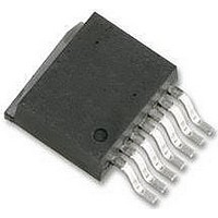
SIMPLESWITH, 3.0A 4.5~42VIN, 7TO263
Manufacturer
National Semiconductor
Datasheet
1.LM22676MR-ADJ.pdf
(16 pages)
Specifications of LM22676TJE-ADJ
Primary Input Voltage
42V
No. Of Outputs
1
Output Current
3A
Voltage Regulator Case Style
TO-263
No. Of Pins
7
Operating Temperature Range
-40°C To +125°C
Svhc
No SVHC (15-Dec-2010)
Package
RoHS Compliant
Available stocks
Company
Part Number
Manufacturer
Quantity
Price

Part Number:
LM22676TJE-ADJ/NOPB
Manufacturer:
TI/德州仪器
Quantity:
20 000


www.national.com
off. The average current into VIN during switch on-time is the
load current. The input capacitance should be selected for
RMS current, I
proximation for the required ripple current rating necessary is
I
Quality ceramic capacitors with a low ESR should be selected
for the input filter. To allow for capacitor tolerances and volt-
age effects, multiple capacitors may be used in parallel. If step
input voltage transients are expected near the maximum rat-
ing of the LM22676, a careful evaluation of ringing and pos-
sible voltage spikes at the VIN pin should be completed. An
additional damping network or input voltage clamp may be
required in these cases.
Usually putting a higher ESR electrolytic input capacitor in
parallel to the low ESR bypass capacitor will help to reduce
excessive voltages during a line transient and will also move
the resonance frequency of the input filter away from the reg-
ulator bandwidth.
Output Capacitor
The output capacitor can limit the output ripple voltage and
provide a source of charge for transient loading conditions.
Multiple capacitors can be placed in parallel. Very low ESR
capacitors such as ceramic capacitors reduce the output rip-
ple voltage and noise spikes, while larger higher ESR capac-
itors in parallel provide large bulk capacitance for transient
loading conditions. An approximation for the output voltage
ripple is:
where ΔI
Cboot Capacitor
The bootstrap capacitor between the BOOT pin and the SW
pin supplies the gate current to turn on the N-channel MOS-
FET. The recommended value of this capacitor is 10 nF and
should be a good quality, low ESR ceramic capacitor.
It is possible to put a small resistor in series with the Cboot
capacitor to slow down the turn-on transition time of the in-
ternal N-channel MOSFET. Resistors in the range of 10Ω to
50Ω can slow down the transition time. This can reduce EMI
of a switched mode power supply circuit. Using such a series
resistor is not recommended for every design since it will in-
crease the switching losses of the application and makes
thermal considerations more challenging.
Resistor Divider
For the -5.0 option no resistor divider is required for 5V output
voltage. The output voltage should be directly connected to
the FB pin. Output voltages above 5V can use the -5.0 option
with a resistor divider as an alternative to the -ADJ option.
This may offer improved loop bandwidth in some applications.
See the Internal Compensation section for more details.
For the -ADJ option no resistor divider is required for 1.285V
output voltage. The output voltage should be directly con-
nected to the FB pin. Other output voltages can use the -ADJ
option with a resistor divider.
The resistor values can be determined by the following equa-
tions:
-ADJ option:
RMS
> I
OUT
L
is the inductor ripple current.
/ 2.
RMS
, and minimum ripple voltage. A good ap-
10
-5.0 option:
Where V
-5.0 option
A maximum value of 10 kΩ is recommended for the sum of
R1 and R2 to keep high output voltage accuracy for the –ADJ
option. A maximum of 2 kΩ is recommended for the -5.0 out-
put voltage option. For the 5V fixed output voltage option, the
total internal divider resistance is typically 9.93 kΩ.
At loads less than 5 mA, the boot capacitor will not hold
enough charge to power the internal high side driver. The
output voltage may droop until the boot capacitor is
recharged. Selecting a total feedback resistance to be below
3 kΩ will provide some minimal load and can keep the output
voltage from collapsing in such low load conditions.
Catch Diode
A Schottky type re-circulating diode is required for all
LM22676 applications. Ultra-fast diodes which are not Schot-
tky diodes are not recommended and may result in damage
to the IC due to reverse recovery current transients. The near
ideal reverse recovery characteristics and low forward volt-
age drop of Schottky diodes are particularly important diode
characteristics for high input voltage and low output voltage
applications common to the LM22676. The reverse recovery
characteristic determines how long the current surge lasts
each cycle when the N-channel MOSFET is turned on. The
reverse recovery characteristics of Schottky diodes mini-
mizes the peak instantaneous power in the switch occurring
during turn-on for each cycle. The resulting switching losses
are significantly reduced when using a Schottky diode. The
reverse breakdown rating should be selected for the maxi-
mum V
a diode with the reverse voltage rating of 1.3 times the max-
imum input voltage.
The forward voltage drop has a significant impact on the con-
version efficiency, especially for applications with a low output
voltage. ‘Rated’ current for diodes varies widely from various
manufacturers. The worst case is to assume a short circuit
load condition. In this case the diode will carry the output cur-
rent almost continuously. For the LM22676 this current can
be as high as 4.2A (typical). Assuming a worst case 1V drop
IN
FB
, plus some safety margin. A rule of thumb is to select
FIGURE 2. Resistive Feedback Divider
= 1.285V typical for the -ADJ option and 5V for the
30076523
Related parts for LM22676TJE-ADJ
Image
Part Number
Description
Manufacturer
Datasheet
Request
R

Part Number:
Description:
IC REG SWITCH BUC 3A ADJ TO263-7
Manufacturer:
National Semiconductor
Datasheet:
Part Number:
Description:
IC REG SWITCH BUCK 3A 5V TO263-7
Manufacturer:
National Semiconductor
Datasheet:

Part Number:
Description:
REGULATOR, ADJ. VOLTAGE, 3A 7TO263
Manufacturer:
National Semiconductor
Datasheet:

Part Number:
Description:
National Semiconductor [8-Bit D/A Converter]
Manufacturer:
National Semiconductor
Datasheet:
Part Number:
Description:
National Semiconductor [Media Coprocessor]
Manufacturer:
National Semiconductor
Datasheet:
Part Number:
Description:
Digitally Controlled Tone and Volume Circuit with Stereo Audio Power Amplifier, Microphone Preamp Stage and National 3D Sound
Manufacturer:
National Semiconductor
Datasheet:
Part Number:
Description:
Digitally Controlled Tone and Volume Circuit with Stereo Audio Power Amplifier, Microphone Preamp Stage and National 3D Sound
Manufacturer:
National Semiconductor
Datasheet:
Part Number:
Description:
AC97 Rev 2 Codec with Sample Rate Conversion and National 3D Sound
Manufacturer:
National Semiconductor
Part Number:
Description:
Manufacturer:
National Semiconductor
Datasheet:
Part Number:
Description:
Manufacturer:
National Semiconductor
Datasheet:
Part Number:
Description:
General Purpose, Low Voltage, Low Power, Rail-to-Rail Output Operational Amplifiers
Manufacturer:
National Semiconductor
Datasheet:
Part Number:
Description:
8-bit 20 MSPS flash A/D converter.
Manufacturer:
National Semiconductor
Datasheet:
Part Number:
Description:
Low Noise Quad Operational Amplifier
Manufacturer:
National Semiconductor
Datasheet:
Part Number:
Description:
Quad Differential Line Receivers
Manufacturer:
National Semiconductor
Datasheet: