LM22676TJE-ADJ National Semiconductor, LM22676TJE-ADJ Datasheet - Page 9
LM22676TJE-ADJ
Manufacturer Part Number
LM22676TJE-ADJ
Description
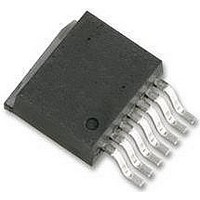
SIMPLESWITH, 3.0A 4.5~42VIN, 7TO263
Manufacturer
National Semiconductor
Datasheet
1.LM22676MR-ADJ.pdf
(16 pages)
Specifications of LM22676TJE-ADJ
Primary Input Voltage
42V
No. Of Outputs
1
Output Current
3A
Voltage Regulator Case Style
TO-263
No. Of Pins
7
Operating Temperature Range
-40°C To +125°C
Svhc
No SVHC (15-Dec-2010)
Package
RoHS Compliant
Available stocks
Company
Part Number
Manufacturer
Quantity
Price

Part Number:
LM22676TJE-ADJ/NOPB
Manufacturer:
TI/德州仪器
Quantity:
20 000


Boot Pin
The LM22676 integrates an N-Channel FET switch and as-
sociated floating high voltage level shift / gate driver. This gate
driver circuit works in conjunction with an internal diode and
an external bootstrap capacitor. A 0.01 µF ceramic capacitor
connected with short traces between the BOOT pin and the
SW pin is recommended to effectively drive the internal FET
switch. During the off-time of the switch, the SW voltage is
approximately -0.5V and the external bootstrap capacitor is
charged from the internal supply through the internal boot-
strap diode. When operating with a high PWM duty-cycle, the
buck switch will be forced off each cycle to ensure that the
bootstrap capacitor is recharged. See the maximum duty-cy-
cle section for more details.
Thermal Protection
Internal Thermal Shutdown circuitry protects the LM22676 in
the event the maximum junction temperature is exceeded.
When activated, typically at 150°C, the regulator is forced into
a low power reset state. There is a typical hysteresis of 15
degrees.
Internal Compensation
The LM22676 has internal compensation designed for a sta-
ble loop with a wide range of external power stage compo-
nents.
Insuring stability of a design with a specific power stage (in-
ductor and output capacitor) can be tricky. The LM22676
stability can be verified over varying loads and input and out-
put voltages using WEBENCH® Designer online circuit sim-
ulation tool at www.national.com. A quick start spreadsheet
can also be downloaded from the online product folder.
The internal compensation of the -ADJ option of the LM22676
is optimized for output voltages below 5V. If an output voltage
of 5V or higher is needed, the -5.0 option with an additional
external resistor divider may also be used.
The typical location of the internal compensation poles and
zeros as well as the DC gain is given in Table 1. The LM22676
has internal type III compensation allowing for the use of most
output capacitors including ceramics.
This information can be used to calculate the transfer function
from the FB pin to the internal compensation node (input to
the PWM comparator in the block diagram).
For the power stage transfer function the standard voltage
mode formulas for the double pole and the ESR zero apply:
Corners
DC gain
Zero 1
Zero 2
Pole 1
Pole 2
Pole 3
TABLE 1.
Frequency
150 kHz
250 kHz
37.5 dB
1.5 kHz
100 Hz
15 kHz
9
The peak ramp level of the oscillator signal feeding into the
PWM comparator is V
this modulator stage of the IC. The -5.0 fixed output voltage
option has twice the gain of the compensation transfer func-
tion compared to the -ADJ option which is 43.5dB instead of
37.5dB.
Generally, calculation as well as simulation can only aid in
selecting good power stage components. A good design prac-
tice is to test for stability with load transient tests or loop
measurement tests. Application note AN-1889 shows how to
easily perform a loop transfer function measurement with only
an oscilloscope and a function generator.
Application Information
EXTERNAL COMPONENTS
The following design procedures can be used to design a non-
synchronous buck converter with the LM22676.
Inductor
The inductor value is determined based on the load current,
ripple current, and the minimum and maximum input voltage.
To keep the application in continuous current conduction
mode (CCM), the maximum ripple current, I
less than twice the minimum load current.
The general rule of keeping the inductor current peak-to-peak
ripple around 30% of the nominal output current is a good
compromise between excessive output voltage ripple and ex-
cessive component size and cost. When selecting the induc-
tor ripple current ensure that the peak current is below the
minimum current limit as given in the Electrical Characteris-
tics section. Using this value of ripple current, the value of
inductor, L, is calculated using the following formula:
where F is the switching frequency which is 500 kHz (typical).
This procedure provides a guide to select the value of the
inductor L. The nearest standard value will then be used in
the circuit.
Increasing the inductance will generally slow down the tran-
sient response but reduce the output voltage ripple amplitude.
Reducing the inductance will generally improve the transient
response but increase the output voltage ripple.
The inductor must be rated for the peak current, I
vent saturation. During normal loading conditions, the peak
current occurs at maximum load current plus maximum ripple.
Under an overload condition as well as during load transients,
the peak current is limited to 4.2A typical (5.5A maximum).
This requires that the inductor be selected such that it can run
at the maximum current limit and not only the steady state
current.
Depending on inductor manufacturer, the saturation rating is
defined as the current necessary for the inductance to reduce
by 30% at 20°C. In typical designs the inductor will run at
higher temperatures. If the inductor is not rated for enough
current, it might saturate and due to the propagation delay of
the current limit circuitry, the power supply may get damaged.
Input Capacitor
Good quality input capacitors are necessary to limit the ripple
voltage at the VIN pin while supplying most of the switch cur-
rent during on-time. When the switch turns on, the current into
the VIN pin steps to the peak value, then drops to zero at turn-
IN
/10 which equals a gain of 20dB of
RIPPLE
www.national.com
, should be
PK+
, to pre-
Related parts for LM22676TJE-ADJ
Image
Part Number
Description
Manufacturer
Datasheet
Request
R

Part Number:
Description:
IC REG SWITCH BUC 3A ADJ TO263-7
Manufacturer:
National Semiconductor
Datasheet:
Part Number:
Description:
IC REG SWITCH BUCK 3A 5V TO263-7
Manufacturer:
National Semiconductor
Datasheet:

Part Number:
Description:
REGULATOR, ADJ. VOLTAGE, 3A 7TO263
Manufacturer:
National Semiconductor
Datasheet:

Part Number:
Description:
National Semiconductor [8-Bit D/A Converter]
Manufacturer:
National Semiconductor
Datasheet:
Part Number:
Description:
National Semiconductor [Media Coprocessor]
Manufacturer:
National Semiconductor
Datasheet:
Part Number:
Description:
Digitally Controlled Tone and Volume Circuit with Stereo Audio Power Amplifier, Microphone Preamp Stage and National 3D Sound
Manufacturer:
National Semiconductor
Datasheet:
Part Number:
Description:
Digitally Controlled Tone and Volume Circuit with Stereo Audio Power Amplifier, Microphone Preamp Stage and National 3D Sound
Manufacturer:
National Semiconductor
Datasheet:
Part Number:
Description:
AC97 Rev 2 Codec with Sample Rate Conversion and National 3D Sound
Manufacturer:
National Semiconductor
Part Number:
Description:
Manufacturer:
National Semiconductor
Datasheet:
Part Number:
Description:
Manufacturer:
National Semiconductor
Datasheet:
Part Number:
Description:
General Purpose, Low Voltage, Low Power, Rail-to-Rail Output Operational Amplifiers
Manufacturer:
National Semiconductor
Datasheet:
Part Number:
Description:
8-bit 20 MSPS flash A/D converter.
Manufacturer:
National Semiconductor
Datasheet:
Part Number:
Description:
Low Noise Quad Operational Amplifier
Manufacturer:
National Semiconductor
Datasheet:
Part Number:
Description:
Quad Differential Line Receivers
Manufacturer:
National Semiconductor
Datasheet: