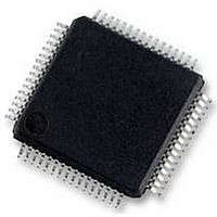
LPC2144FBD64 NXP Semiconductors, LPC2144FBD64 Datasheet - Page 21

LPC2144FBD64
Manufacturer Part Number
LPC2144FBD64
Description
MCU 32BIT ARM7 128K FLASH, LQFP64
Manufacturer
NXP Semiconductors
Datasheet
1.LPC2142FBD64.pdf
(40 pages)
Specifications of LPC2144FBD64
Core Size
32bit
No. Of I/o's
45
Program Memory Size
128KB
Ram Memory Size
16KB
Cpu Speed
60MHz
Oscillator Type
External Only
No. Of Timers
2
No. Of Pwm Channels
6
Digital Ic Case Style
LQFP
Controller Family/series
LPC21xx
Peripherals
ADC,
Rohs Compliant
Yes
Lead Free Status / RoHS Status
Lead free / RoHS Compliant
Available stocks
Company
Part Number
Manufacturer
Quantity
Price
Company:
Part Number:
LPC2144FBD64
Manufacturer:
NXP
Quantity:
1 082
Part Number:
LPC2144FBD64
Manufacturer:
NXP/恩智浦
Quantity:
20 000
Company:
Part Number:
LPC2144FBD64,151
Manufacturer:
IR
Quantity:
12 000
Company:
Part Number:
LPC2144FBD64,151
Manufacturer:
NXP Semiconductors
Quantity:
10 000
NXP Semiconductors
LPC2141_42_44_46_48_4
Product data sheet
6.18.1 Features
6.18 Pulse width modulator
The PWM is based on the standard timer block and inherits all of its features, although
only the PWM function is pinned out on the LPC2141/42/44/46/48. The timer is designed
to count cycles of the peripheral clock (PCLK) and optionally generate interrupts or
perform other actions when specified timer values occur, based on seven match registers.
The PWM function is also based on match register events.
The ability to separately control rising and falling edge locations allows the PWM to be
used for more applications. For instance, multi-phase motor control typically requires three
non-overlapping PWM outputs with individual control of all three pulse widths and
positions.
Two match registers can be used to provide a single edge controlled PWM output. One
match register (MR0) controls the PWM cycle rate, by resetting the count upon match.
The other match register controls the PWM edge position. Additional single edge
controlled PWM outputs require only one match register each, since the repetition rate is
the same for all PWM outputs. Multiple single edge controlled PWM outputs will all have a
rising edge at the beginning of each PWM cycle, when an MR0 match occurs.
Three match registers can be used to provide a PWM output with both edges controlled.
Again, the MR0 match register controls the PWM cycle rate. The other match registers
control the two PWM edge positions. Additional double edge controlled PWM outputs
require only two match registers each, since the repetition rate is the same for all PWM
outputs.
With double edge controlled PWM outputs, specific match registers control the rising and
falling edge of the output. This allows both positive going PWM pulses (when the rising
edge occurs prior to the falling edge), and negative going PWM pulses (when the falling
edge occurs prior to the rising edge).
•
•
•
•
•
Seven match registers allow up to six single edge controlled or three double edge
controlled PWM outputs, or a mix of both types.
The match registers also allow:
– Continuous operation with optional interrupt generation on match.
– Stop timer on match with optional interrupt generation.
– Reset timer on match with optional interrupt generation.
Supports single edge controlled and/or double edge controlled PWM outputs. Single
edge controlled PWM outputs all go HIGH at the beginning of each cycle unless the
output is a constant LOW. Double edge controlled PWM outputs can have either edge
occur at any position within a cycle. This allows for both positive going and negative
going pulses.
Pulse period and width can be any number of timer counts. This allows complete
flexibility in the trade-off between resolution and repetition rate. All PWM outputs will
occur at the same repetition rate.
Double edge controlled PWM outputs can be programmed to be either positive going
or negative going pulses.
Rev. 04 — 17 November 2008
LPC2141/42/44/46/48
Single-chip 16-bit/32-bit microcontrollers
© NXP B.V. 2008. All rights reserved.
21 of 40


