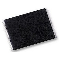
SST39VF1681-70-4C-EKE SILICON STORAGE TECHNOLOGY, SST39VF1681-70-4C-EKE Datasheet - Page 15

SST39VF1681-70-4C-EKE
Manufacturer Part Number
SST39VF1681-70-4C-EKE
Description
IC, 16M FLASH MEMORY, 2KWORD SECTOR
Manufacturer
SILICON STORAGE TECHNOLOGY
Datasheet
1.SST39VF1681-70-4C-EKE.pdf
(29 pages)
Specifications of SST39VF1681-70-4C-EKE
Memory Size
16Mbit
Supply Voltage Range
2.7V To 3.6V
Memory Case Style
TSOP
No. Of Pins
48
Svhc
No SVHC (18-Jun-2010)
Access Time
70ns
Interface
X8 MPF+
Memory Configuration
2M X 8bit
Memory Type
Flash - NOR
Interface Type
CFI
Rohs Compliant
Yes
Lead Free Status / RoHS Status
Lead free / RoHS Compliant
Available stocks
Company
Part Number
Manufacturer
Quantity
Price
Company:
Part Number:
SST39VF1681-70-4C-EKE
Manufacturer:
SST
Quantity:
106
16 Mbit Multi-Purpose Flash Plus
SST39VF1681 / SST39VF1682
©2003 Silicon Storage Technology, Inc.
FIGURE 7: T
FIGURE 8: WE# C
ADDRESS A MS-0
ADDRESS A MS-0
DQ
6
and DQ
Note: This device also supports CE# controlled Chip-Erase operation.
DQ 7-0
WE#
CE#
OE#
WE#
OE#
CE#
OGGLE
The WE# and CE# signals are interchangeable as long as minimum timings are meet. (See Table 15.)
A
A
WP# must be held in proper logic state (V
X can be V
2
MS
MS
= Most Significant Address
= A
ONTROLLED
20
B
ITS
for SST39VF168x
IL
AAA
Note: A
or V
T
T WP
SW0
AA
IMING
IH,
A
but no other value.
MS
MS
C
= A
HIP
T OEH
D
= Most Significant Address
555
IAGRAM
SW1
20
-E
55
for SST39VF168x
RASE
SIX-BYTE CODE FOR CHIP-ERASE
AAA
T
SW2
IMING
T CE
80
T OE
IL
or V
D
AAA
IH
15
IAGRAM
) 1 µs prior to and 1 µs after the command sequence.
SW3
AA
555
SW4
55
AAA
SW5
10
WITH SAME OUTPUTS
TWO READ CYCLES
Preliminary Specifications
T SCE
S71243-03-000
1243 F06.0
1243 F07.0
T OES
11/03


