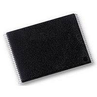
S29AL016D70TFI010 Spansion Inc., S29AL016D70TFI010 Datasheet - Page 24

S29AL016D70TFI010
Manufacturer Part Number
S29AL016D70TFI010
Description
Flash Memory IC
Manufacturer
Spansion Inc.
Datasheet
1.S29AL016D70TFI010.pdf
(58 pages)
Specifications of S29AL016D70TFI010
Memory Size
16Mbit
Memory Configuration
2M X 8 / 1M X 16
Ic Interface Type
Parallel
Access Time
70ns
Memory Case Style
TSOP
No. Of Pins
48
Operating Temperature Range
-40°C To +85°C
Lead Free Status / RoHS Status
Lead free / RoHS Compliant
Available stocks
Company
Part Number
Manufacturer
Quantity
Price
Company:
Part Number:
S29AL016D70TFI010
Manufacturer:
SPANSION
Quantity:
27 880
Part Number:
S29AL016D70TFI010F
Manufacturer:
SPANSION
Quantity:
20 000
Company:
Part Number:
S29AL016D70TFI010H
Manufacturer:
SPANSION
Quantity:
2 890
Company:
Part Number:
S29AL016D70TFI010H
Manufacturer:
SPANSLON
Quantity:
2 115
Part Number:
S29AL016D70TFI010H
Manufacturer:
SPANSION
Quantity:
20 000
NOTE: See
24
Table 9
Unlock Bypass Command Sequence
The unlock bypass feature allows the system to program bytes or words to the
device faster than using the standard program command sequence. The unlock
bypass command sequence is initiated by first writing two unlock cycles. This is
followed by a third write cycle containing the unlock bypass command, 20h. The
device then enters the unlock bypass mode. A two-cycle unlock bypass program
command sequence is all that is required to program in this mode. The first cycle
in this sequence contains the unlock bypass program command, A0h; the second
cycle contains the program address and data. Additional data is programmed in
the same manner. This mode dispenses with the initial two unlock cycles required
in the standard program command sequence, resulting in faster total program-
ming time.
During the unlock bypass mode, only the Unlock Bypass Program and Unlock By-
pass Reset commands are valid. To exit the unlock bypass mode, the system
must issue the two-cycle unlock bypass reset command sequence. The first cycle
must contain the data 90h; the second cycle the data 00h. Addresses are don’t
care for both cycles. The device then returns to reading array data.
Figure 3
gram Operations
timing diagrams.
for program command sequence.
illustrates the algorithm for the program operation. See the
Table 9
Increment Address
table in
shows the requirements for the command sequence.
Figure 3. Program Operation
AC Characteristics
in progress
Embedded
algorithm
Program
S29AL016D
P r e l i m i n a r y
No
Command Sequence
for parameters, and to
Write Program
Last Address?
Programming
from System
Verify Data?
Completed
Data Poll
START
Yes
Yes
No
Figure 17
Erase/Pro-
S29AL016D_00_A2 December 17, 2004
for


