EVAL-ADF4106EBZ1 Analog Devices Inc, EVAL-ADF4106EBZ1 Datasheet - Page 4
EVAL-ADF4106EBZ1
Manufacturer Part Number
EVAL-ADF4106EBZ1
Description
ADF4106 Evaluation Board
Manufacturer
Analog Devices Inc
Datasheet
1.ADF4106BCPZ.pdf
(24 pages)
Specifications of EVAL-ADF4106EBZ1
Silicon Manufacturer
Analog Devices
Application Sub Type
PLL Frequency Synthesizer
Kit Application Type
Clock & Timing
Silicon Core Number
ADF4106
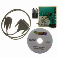
Kit Contents
Board Including Synthesizer, Cables
Main Purpose
Timing, Frequency Synthesizer
Embedded
No
Utilized Ic / Part
ADF4106
Primary Attributes
Single Integer-N PLL
Secondary Attributes
6GHz, Graphical User Interface
Lead Free Status / RoHS Status
Lead free / RoHS Compliant


ADF4106
Parameter
NOISE CHARACTERISTICS
1
2
3
4
5
6
7
8
9
10
11
12
13
14
15
TIMING CHARACTERISITICS
AV
unless otherwise noted.
Table 2.
Parameter
t
t
t
t
t
t
1
1
2
3
4
5
6
Operating temperature range (B Version) is –40°C to +85°C.
The B chip specifications are given as typical values.
This is the maximum operating frequency of the CMOS counters. The prescaler value should be chosen to ensure that the RF input is divided down to a frequency that
is less than this value.
AV
AC coupling ensures AV
Guaranteed by design. Sample tested to ensure compliance.
T
T
T
value) and 10 log F
the synthesizer (f
Operating temperature range (B Version) is –40°C to +85°C.
T
The synthesizer phase noise floor is estimated by measuring the in-band phase noise at the output of the VCO and subtracting 20 log N (where N is the N divider
The phase noise is measured with the EVAL-ADF4106EB1 evaluation board and the Agilent E4440A Spectrum Analyzer. The spectrum analyzer provides the REFIN for
f
f
f
A
A
A
REFIN
REFIN
REFIN
ADF4106 Normalized
Phase Noise Performance
Spurious Signals
A
= 25°C; AV
= 25°C; AV
= 25°C; AV
DD
DD
= 25°C; AV
Phase Noise Floor
900 MHz
5800 MHz
5800 MHz
900 MHz
5800 MHz
5800 MHz
= DV
= 10 MHz; f
= 10 MHz; f
= 10 MHz; f
= DV
DD
= 3 V.
DD
DD
DD
DD
DD
13
13
= DV
= DV
= DV
= 3 V ± 10%, AV
= DV
PFD
PFD
PFD
14
15
14
15
REFOUT
PFD
= 200 kHz; Offset Frequency = 1 kHz; f
= 200 kHz; Offset Frequency = 1 kHz; f
= 1 MHz; Offset Frequency = 1 kHz; f
DD
DD
DD
DD
. PN
= 10 MHz @ 0 dBm).
= 3 V; P = 16; RF
= 3 V; P = 16; RF
= 3 V; P = 32; RF
= 3.3 V; R = 16383; A = 63; B = 891; P = 32; RF
DD
SYNTH
/2 bias.
11
= PN
CLOCK
12
DATA
TOT
LE
LE
DD
− 10 log F
IN
IN
IN
≤ V
= 900 MHz.
= 2.0 GHz.
= 6.0 GHz.
DB23 (MSB)
Limit
10
10
25
25
10
20
P
≤ 5.5 V, AGND = DGND = CPGND = 0 V, R
PFD
B Version
–219
–92.5
−76.5
−83.5
–90/–92
–65/–70
–70/–75
1
(B Version)
− 20 log N.
RF
RF
RF
= 5800 MHz; N = 5800; Loop B/W = 100 kHz.
t
1
= 900 MHz; N = 4500; Loop B/W = 20 kHz.
= 5800 MHz; N = 29000; Loop B/W = 20 kHz.
1
DB22
B Chips
–219
−92.5
−76.5
−83.5
–90/–92
–65/–70
–70/–75
t
2
IN
= 6.0 GHz.
Figure 2. Timing Diagram
Rev. C | Page 4 of 24
2
(typ)
DB2
Unit
ns min
ns min
ns min
ns min
ns min
ns min
t
3
Unit
dBc/Hz typ
dBc/Hz typ
dBc/Hz typ
dBc/Hz typ
dBc typ
dBc typ
dBc typ
DB1 (CONTROL
t
4
BIT C2)
Test Conditions/Comments
DATA to CLOCK Setup Time
DATA to CLOCK Hold Time
CLOCK High Duration
CLOCK Low Duration
CLOCK to LE Setup Time
LE Pulse Width
SET
= 5.1 kΩ, dBm referred to 50 Ω, T
(CONTROL BIT C1)
Test Conditions/Comments
@ VCO output
@ 1 kHz offset and 200 kHz PFD frequency
@ 1 kHz offset and 200 kHz PFD frequency
@ 1 kHz offset and 1 MHz PFD frequency
@ 200 kHz/400 kHz and 200 kHz PFD frequency
@ 200 kHz/400 kHz and 200 kHz PFD frequency
@ 1 MHz/2 MHz and 1 MHz PFD frequency
t
5
DB0 (LSB)
t
6
A
= T
MAX
to T
MIN
,
Related parts for EVAL-ADF4106EBZ1
Image
Part Number
Description
Manufacturer
Datasheet
Request
R

Part Number:
Description:
IC, ADJ LDO REG, 1.5V TO 5V 250mA MSOP-8
Manufacturer:
Vishay
Datasheet:

Part Number:
Description:
IC, ADJ LDO REG, 1.5V TO 5V 0.6A 8-TSSOP
Manufacturer:
Vishay
Datasheet:
Part Number:
Description:
IC, ADJ LDO REG, 1.5V TO 5V 250mA MSOP-8
Manufacturer:
Vishay
Datasheet:

Part Number:
Description:
IC ADJ LDO REG 1.5V TO 5V 150mA 5-SOT-23
Manufacturer:
Vishay
Datasheet:

Part Number:
Description:
BOARD EVAL AS1324-AD
Manufacturer:
austriamicrosystems
Datasheet:
Part Number:
Description:
IC, ADJ LDO REG, 1.5V TO 5V 0.6A 8-TSSOP
Manufacturer:
Vishay
Datasheet:

Part Number:
Description:
IC, ADJ LDO REG, 1.5V TO 5V, 0.3A, MSOP8
Manufacturer:
Vishay
Datasheet:
Part Number:
Description:
IC, ADJ LDO REG, 1.5V TO 5V, 0.3A, MSOP8
Manufacturer:
Vishay
Datasheet:
Part Number:
Description:
IC, ADJ LDO REG 1.215V TO 5V 0.3A MSOP-8
Manufacturer:
Vishay
Datasheet:
Part Number:
Description:
IC, ADJ LDO REG 1.215V TO 5V 0.3A MSOP-8
Manufacturer:
Vishay
Datasheet:

Part Number:
Description:
±1.7g Dual-Axis IMEMS Accelerometer Evaluation Board
Manufacturer:
Analog Devices Inc
Datasheet:

Part Number:
Description:
IC MULTIPLIER ANALOG 8-SOIC T/R
Manufacturer:
Analog Devices Inc
Datasheet:

Part Number:
Description:
IC ANALOG MULTIPLIER 8-DIP
Manufacturer:
Analog Devices Inc
Datasheet:
Part Number:
Description:
IC ANALOG MULTIPLIER 8-SOIC
Manufacturer:
Analog Devices Inc
Datasheet:
Part Number:
Description:
IC ANALOG MULTIPLIER 8-DIP
Manufacturer:
Analog Devices Inc
Datasheet: