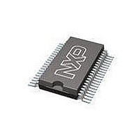
PCF2111CTD NXP Semiconductors, PCF2111CTD Datasheet - Page 9

PCF2111CTD
Manufacturer Part Number
PCF2111CTD
Description
LCD Drivers LCD DRIVER 64 SEG
Manufacturer
NXP Semiconductors
Datasheet
1.PCF2100CTF1112.pdf
(24 pages)
Specifications of PCF2111CTD
Number Of Segments
64
Operating Supply Voltage
2.25 V to 6 V
Maximum Power Dissipation
500 mW
Maximum Operating Temperature
+ 85 C
Package / Case
VSO-40
Maximum Supply Current
50 uA
Minimum Operating Temperature
- 40 C
Lead Free Status / RoHS Status
Lead free / RoHS Compliant
Other names
PCF2111CT/1,112
Philips Semiconductors
7
An LCD segment or LED output is activated when the
corresponding DATA bit is HIGH.
7.1
When DATA bit 21 is HIGH, the A-latches (BP1) are
loaded. With DATA bit 21 LOW, the B-latches (BP2) are
loaded. CLB pulse 23 transfers data from the shift register
to the selected latches.
7.2
When DATA bit 33 is HIGH, the A-latches (BP1) are
loaded. With DATA bit 33 LOW, the B-latches (BP2) are
loaded. CLB pulse 35 transfers data from the shift register
to the selected latches.
1997 Mar 28
handbook, full pagewidth
LCD drivers
FUNCTIONAL DESCRIPTION
DLEN
DATA
PCF2100C
PCF2111C
CLB
bit number
output
test leading zero
leading zero
1
0
2
S1
S1
1
1
3
S2
S2
2
2
4
S3
S3
3
3
5
S4
S4
4
4
6
S5
S5
5
5
Fig.7 CBUS data format.
7
S6
S6
6
6
8
S7
S7
7
7
9
7.3
When DATA bit 33 is HIGH, the latches are loaded.
CLB pulse 35 transfers data from the shift register to the
selected latches.
7.4
The following tests are carried out by the bus control logic:
1. Test on leading zero
2. Test on number of DATA bits
3. Test of disturbed DLEN and DATA signals during
If one of the test conditions is not fulfilled, no action follows
the load condition (load pulse with DLEN LOW) and the
driver is ready to receive new data.
transmission.
32
20
S31
S19
31
19
PCF2112C
Bus control logic
33
21
S32
S20
32
20
load bit
34
22
33
21
load pulse
35
23
PCF2111C and PCF2112C
PCF2100C
PCF21xxC family
PCF2111C and PCF2112C
PCF2100C
Product specification
MLD296


