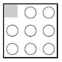
IP4064CX8/LF,135 NXP Semiconductors, IP4064CX8/LF,135 Datasheet

IP4064CX8/LF,135
Specifications of IP4064CX8/LF,135
Related parts for IP4064CX8/LF,135
IP4064CX8/LF,135 Summary of contents
Page 1
IP4064CX8/LF; IP4364CX8/LF Integrated SIM card passive filter array with ESD protection to IEC61000-4-2, level 4 Rev. 01 — 12 November 2007 1. Product profile 1.1 General description The IP4064CX8/LF and IP4364CX8/LF are 3-channel RC low-pass filter arrays which are designed ...
Page 2
... NXP Semiconductors 2. Pinning information 2.1 Pinning Fig 1. Pin configuration IP4064CX8/LF 2.2 Pin description Table 1. Pin Ordering information Table 2. Ordering information Type number Package Name IP4064CX8/LF WLCSP8 IP4364CX8/LF WLCSP8 IP4064CX8LF_IP4364CX8LF_1 Product data sheet IP4064CX8/LF; IP4364CX8/LF Integrated SIM card passive filter array with ESD protection ...
Page 3
... NXP Semiconductors 4. Functional diagram Fig 3. Schematic diagram IP4064CX8/LF and IP4364CX8/LF 5. Limiting values Table 3. In accordance with the Absolute Maximum Rating System (IEC 60134). Symbol ESD tot T stg T reflow(peak) T amb [1] Device is tested with 1000 pulses contact discharges each, according the IEC61000-4-2 model and so exceeds the specifi ...
Page 4
... NXP Semiconductors 6. Characteristics Table unless otherwise specified. amb Symbol Parameter R s(ch IP4064CX8LF_IP4364CX8LF_1 Product data sheet IP4064CX8/LF; IP4364CX8/LF Integrated SIM card passive filter array with ESD protection Characteristics Conditions channel series resistance R1 channel capacitance including diode capacitance MHz breakdown voltage test ...
Page 5
... NXP Semiconductors 7. Application information 7.1 Insertion loss The IP4064CX8/LF and IP4364CX8/LF is mainly designed as an EMI/RFI filter for SIM card interfaces. The insertion loss IP4364CX8/LF is shown in identical. The insertion loss of the three channels was measured with a test PCB utilizing laser drilled micro-via holes that connect the PCB ground plane to the ground pins. ...
Page 6
... NXP Semiconductors 7.2 Crosstalk The set-up for crosstalk measurements shown in in Figure with 50 Fig 6. Crosstalk measurement configuration (1) Pin C1 to B3. (2) Pin B1 to C3. (3) Pin B1 to A3. (4) Pin A2 to C3. Fig 7. Typical IP4064CX8/LF and IP4364CX8/LF crosstalk behavior IP4064CX8LF_IP4364CX8LF_1 Product data sheet IP4064CX8/LF; IP4364CX8/LF Integrated SIM card passive fi ...
Page 7
... NXP Semiconductors 8. Package outline WLCSP8: wafer level chip-size package; 8 bumps; 1.41 x 1.41 x 0.7 mm bump A1 index area DIMENSIONS (mm are the original dimensions) A UNIT max 0.26 0.44 0.37 mm 0.7 0.22 0.38 0.27 OUTLINE VERSION IEC IP4064CX8/LF Fig 8. Package outline IP4064CX8/LF (WLCSP8) IP4064CX8LF_IP4364CX8LF_1 Product data sheet IP4064CX8/LF ...
Page 8
... NXP Semiconductors WLCSP8: wafer level chip-size package; 8 bumps; 1.16 x 1.16 x 0.66 mm bump A1 index area DIMENSIONS (mm are the original dimensions) A UNIT max 0.22 0.44 0.31 mm 0.66 0.18 0.38 0.21 OUTLINE VERSION IEC IP4364CX8/LF Fig 9. Package outline IP4364CX8/LF (WLCSP8) IP4064CX8LF_IP4364CX8LF_1 Product data sheet IP4064CX8/LF ...
Page 9
... NXP Semiconductors 9. Soldering 9.1 Introduction to soldering WLCSP packages This text provides a very brief insight into a complex technology. A more in-depth account of soldering WLCSP (Wafer Level Chip-Size Packages) can be found in application note AN10439 “Wafer Level Chip Scale Package” and in application note AN10365 “Surface mount refl ...
Page 10
... NXP Semiconductors Fig 10. Temperature profiles for large and small components For further information on temperature profiles, refer to application note AN10365 “Surface mount reflow soldering description” . 9.3.1 Stand off The stand off between the substrate and the chip is determined by: • ...
Page 11
... NXP Semiconductors Device removal can be done when the substrate is heated until it is certain that all solder joints are molten. The chip can then be carefully removed from the substrate without damaging the tracks and solder lands on the substrate. Removing the device must be done using plastic tweezers, because metal tweezers can damage the silicon. The surface of the substrate should be carefully cleaned and all solder and fl ...
Page 12
... Right to make changes — NXP Semiconductors reserves the right to make changes to information published in this document, including without limitation specifications and product descriptions, at any time and without notice ...
Page 13
... NXP Semiconductors 14. Contents 1 Product profi 1.1 General description 1.2 Features . . . . . . . . . . . . . . . . . . . . . . . . . . . . . . 1 1.3 Applications . . . . . . . . . . . . . . . . . . . . . . . . . . . 1 2 Pinning information . . . . . . . . . . . . . . . . . . . . . . 2 2.1 Pinning . . . . . . . . . . . . . . . . . . . . . . . . . . . . . . . 2 2.2 Pin description . . . . . . . . . . . . . . . . . . . . . . . . . 2 3 Ordering information . . . . . . . . . . . . . . . . . . . . . 2 4 Functional diagram . . . . . . . . . . . . . . . . . . . . . . 3 5 Limiting values Characteristics . . . . . . . . . . . . . . . . . . . . . . . . . . 4 7 Application information 7.1 Insertion loss . . . . . . . . . . . . . . . . . . . . . . . . . . 5 7.2 Crosstalk Package outline . . . . . . . . . . . . . . . . . . . . . . . . . 7 9 Soldering ...


