EA-EDU-010 Embedded Artists, EA-EDU-010 Datasheet
EA-EDU-010
Specifications of EA-EDU-010


Related parts for EA-EDU-010


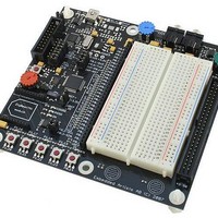
EA-EDU-010 Summary of contents
Page 1
... Enhancements brought by LPC213x/01 devices Fast GPIO ports enable port pin toggling up to 3.5 times faster than the original LPC213x. They also allow for a port pin to be read at any time regardless of its function. Dedicated result registers for ADC(s) reduce interrupt overhead. ...
Page 2
... Two 32-bit timers/external event counters (with four capture and four compare channels each), PWM unit (six outputs) and watchdog. Low power Real-time clock with independent power and dedicated 32 kHz clock input. Multiple serial interfaces including two UARTs (16C550), two Fast I SPI and SSP with buffering and variable data length capabilities. ...
Page 3
... LQFP64 plastic low profile quad flat package; 64 leads; body 10 × 10 × 1.4 mm plastic low profile quad flat package; 64 leads; body 10 × 10 × 1.4 mm HVQFN64 plastic thermal enhanced very thin quad flat package; no leads; 64 terminals; body 9 × 9 × 0.85 mm package ...
Page 4
... SYSTEM PLL FUNCTIONS system VECTORED clock INTERRUPT CONTROLLER AMBA AHB AHB DECODER APB SERIAL INTERFACES 0 AND 1 SPI AND SSP SERIAL INTERFACES UART0/UART1 REAL TIME CLOCK WATCHDOG TIMER SYSTEM CONTROL 002aab067 SCL0,1 SDA0,1 SCK0,1 MOSI0,1 MISO0,1 SSEL0,1 TXD0,1 RXD0,1 (1) (1) DSR1 ,CTS1 (1) ...
Page 5
NXP Semiconductors 5. Pinning information 5.1 Pinning P0.21/PWM5/CAP1 P0.22/CAP0.0/MAT0.0 RTCX1 3 P1.19/TRACEPKT3 4 RTCX2 DDA P1.18/TRACEPKT2 8 P0.25/AD0.4 9 P0.26/AD0.5 10 P0.27/AD0.0/CAP0.1/MAT0 P1.17/TRACEPKT1 13 P0.28/AD0.1/CAP0.2/MAT0.2 P0.29/AD0.2/CAP0.3/MAT0.3 14 P0.30/AD0.3/EINT3/CAP0.0 15 P1.16/TRACEPKT0 ...
Page 6
NXP Semiconductors P0.21/PWM5/CAP1.3 1 P0.22/CAP0.0/MAT0.0 2 RTCX1 3 P1.19/TRACEPKT3 4 5 RTCX2 DDA P1.18/TRACEPKT2 8 P0.25/AD0.4/AOUT 9 10 P0.26/AD0.5 P0.27/AD0.0/CAP0.1/MAT0.1 11 P1.17/TRACEPKT1 12 P0.28/AD0.1/CAP0.2/MAT0.2 13 P0.29/AD0.2/CAP0.3/MAT0 P0.30/AD0.3/EINT3/CAP0.0 16 P1.16/TRACEPKT0 Fig 3. LPC2132 LQFP64 ...
Page 7
NXP Semiconductors P0.21/PWM5/AD1.6/CAP1.3 1 P0.22/AD1.7/CAP0.0/MAT0.0 2 RTCX1 3 P1.19/TRACEPKT3 4 5 RTCX2 DDA P1.18/TRACEPKT2 8 P0.25/AD0.4/AOUT 9 10 P0.26/AD0.5 P0.27/AD0.0/CAP0.1/MAT0.1 11 P1.17/TRACEPKT1 12 P0.28/AD0.1/CAP0.2/MAT0.2 13 P0.29/AD0.2/CAP0.3/MAT0 P0.30/AD0.3/EINT3/CAP0.0 16 P1.16/TRACEPKT0 Fig 4. LPC2134/36/38 LQFP64 ...
Page 8
... NXP Semiconductors terminal 1 index area P0.21/PWM5/AD1.6/CAP1.3 P0.22/AD1.7/CAP0.0/MAT0.0 RTCX1 P1.19/TRACEPKT3 RTCX2 DDA P1.18/TRACEPKT2 P0.25/AD0.4/AOUT P0.26/AD0.5 P0.27/AD0.0/CAP0.1/MAT0.1 P1.17/TRACEPKT1 P0.28/AD0.1/CAP0.2/MAT0.2 P0.29/AD0.2/CAP0.3/MAT0.3 P0.30/AD0.3/EINT3/CAP0.0 P1.16/TRACEPKT0 AD1.7 to AD1.0 only available on LPC2134/36/38. Fig 5. LPC2132/38 HVQFN64 pin configuration LPC2131_32_34_36_38 Product data sheet LPC2132/2138 Transparent top view All information provided in this document is subject to legal disclaimers. ...
Page 9
... Product data sheet Description Port 0: Port 32-bit I/O port with individual direction controls for each bit. Total of 31 pins of the Port 0 can be used as a general purpose bidirectional digital I/Os while P0.31 is output only pin. The operation of port 0 pins depends upon the pin function selected via the pin connect block ...
Page 10
... AD1.3 — ADC 1, input 3. This analog input is always connected to its pin. Available in LPC2134/36/38 only. DTR1 — Data Terminal Ready output for UART1. Available in LPC2134/36/38. MAT1.1 — Match output for Timer 1, channel 1. AD1.4 — ADC 1, input 4. This analog input is always connected to its pin. Available in LPC2134/36/38 only. DCD1 — ...
Page 11
... Important: This pin MUST NOT be externally pulled LOW when RESET pin is LOW or the JTAG port will be disabled. Port 1: Port 32-bit bidirectional I/O port with individual direction controls for each bit. The operation of port 1 pins depends upon the pin function selected via the pin connect block. Pins 0 through 15 of port 1 are not available. TRACEPKT0 — ...
Page 12
... V tolerant pad providing digital input (with TTL levels and hysteresis) function only. [8] Pad provides special analog functionality. [9] When unused, the RTCX1 pin can be grounded or left floating. For lowest power leave it floating. The other RTC pin, RTCX2, should be left floating. LPC2131_32_34_36_38 Product data sheet Description RTCK — ...
Page 13
... Programming of the flash memory may be accomplished in several ways. It may be programmed In System via the serial port. The application program may also erase and/or program the flash while the application is running, allowing a great degree of flexibility for data storage field firmware upgrades, etc. When the LPC2131/32/34/36/38 on-chip bootloader is used, 32/64/128/256/500 kB of flash memory is available for user code ...
Page 14
NXP Semiconductors 6.4 Memory map The LPC2131/32/34/36/38 memory map incorporates several distinct regions, as shown in Figure In addition, the CPU interrupt vectors may be re-mapped to allow them to reside in either flash memory (the default) or on-chip static ...
Page 15
... FIQ latency is achieved when only one request is classified as FIQ, because then the FIQ service routine can simply start dealing with that device. But if more than one request is assigned to the FIQ class, the FIQ service routine can read a word from the VIC that identifies which FIQ source(s) is (are) requesting an interrupt. ...
Page 16
... Device pins that are not connected to a specific peripheral function are controlled by the GPIO registers. Pins may be dynamically configured as inputs or outputs. Separate registers allow setting or clearing any number of outputs simultaneously. The value of the output register may be read back, as well as the current state of the port pins. 6.7.1 Features • ...
Page 17
... Entire port value can be written in one instruction. • Mask registers allow single instruction to set or clear any number of bits in one port. 6.8 10-bit ADC The LPC2131/32 contain one and the LPC2134/36/38 contain two ADCs. These converters are single 10-bit successive approximation ADCs with eight multiplexed channels ...
Page 18
... The I C-bus is bidirectional, for inter-IC control using only two wires: a serial clock line (SCL), and a serial data line (SDA). Each device is recognized by a unique address and can operate as either a receiver-only device (e.g., an LCD driver or a transmitter with the capability to both receive and send information (such as memory)). Transmitters and/or receivers can operate in either master or slave mode, depending on whether the chip has to initiate a data transfer or is only addressed ...
Page 19
... Maximum data bit rate of one eighth of the input clock rate. 6.13 SSP serial I/O controller The LPC2131/32/34/36/38 each contain one Serial Synchronous Port controller (SSP). The SSP controller is capable of operation on a SPI, 4-wire SSI, or Microwire bus. It can interact with multiple masters and slaves on the bus. However, only a single master and a single slave can communicate on the bus during a given data transfer ...
Page 20
... Do nothing on match. 6.15 Watchdog timer The purpose of the watchdog is to reset the microcontroller within a reasonable amount of time if it enters an erroneous state. When enabled, the watchdog will generate a system reset if the user program fails to ‘feed’ (or reload) the watchdog within a predetermined amount of time ...
Page 21
... Again, the MR0 match register controls the PWM cycle rate. The other match registers control the two PWM edge positions. Additional double edge controlled PWM outputs require only two match registers each, since the repetition rate is the same for all PWM outputs. ...
Page 22
... This is important at power on, all types of reset, and whenever any of the aforementioned functions are turned off for any reason. Since the oscillator and other functions are turned off during Power-down mode, any wake-up of the processor from Power-down mode makes use of the wake-up timer ...
Page 23
... NXP Semiconductors The wake-up timer monitors the crystal oscillator as the means of checking whether it is safe to begin code execution. When power is applied to the chip, or some event caused the chip to exit Power-down mode, some time is required for the oscillator to produce a signal of sufficient amplitude to drive the clock logic. The amount of time depends on ...
Page 24
... Power-down mode reduces chip power consumption to nearly zero. Selecting an external 32 kHz clock instead of the PCLK as a clock-source for the on-chip RTC will enable the microcontroller to have the RTC active during Power-down mode. Power-down current is increased with RTC active. However significantly lower than in Idle mode ...
Page 25
... RealMonitor RealMonitor is a configurable software module, developed by ARM Inc., which enables real time debug lightweight debug monitor that runs in the background while users debug their foreground application. It communicates with the host using the DCC, which is present in the EmbeddedICE logic. The LPC2131/32/34/36/38 contain a specific configuration of RealMonitor software programmed into the on-chip flash memory ...
Page 26
... The following applies to the Limiting values: a) This product includes circuitry specifically designed for the protection of its internal devices from the damaging effects of excessive static charge. Nonetheless suggested that conventional precautions be taken to avoid applying greater than the rated maximum. b) Parameters are valid over operating temperature range unless otherwise specified. All voltages are with respect to V otherwise noted ...
Page 27
NXP Semiconductors 8. Static characteristics Table 6. Static characteristics − ° ° +85 C for commercial applications, unless otherwise specified. amb Symbol Parameter V supply voltage (core and DD external rail) V analog 3.3 V ...
Page 28
... I C-bus pins V HIGH-level input voltage IH V LOW-level input voltage IL V hysteresis voltage hys V LOW-level output voltage OL I input leakage current LI Oscillator pins V input voltage on pin i(XTAL1) XTAL1 V output voltage on pin o(XTAL2) XTAL2 V input voltage on pin i(RTCX1) RTCX1 V output voltage on pin ...
Page 29
... V supply voltages must be present. DD [5] 3-state outputs go into 3-state mode when V [6] Please also see the errata note mentioned in the errata sheet. [7] Accounts for 100 mV voltage drop in all supply lines. [8] Only allowed for a short time period. [9] Minimum condition for V = 4.5 V, maximum condition for V I [10] Applies to P1 ...
Page 30
... NXP Semiconductors 9.1 Timing Fig 7. External clock timing (with an amplitude of at least V 9.2 LPC2138 power consumption measurements 40 I (mA Test conditions: code executed from flash; all peripherals are enabled in PCONP register; PCLK = CCLK/ −60 °C (max 140 ° ° °C (typical °C (typical) ...
Page 31
... −60 ° ° °C (typical °C (typical) ( Fig 9. I idle measured at different frequencies (CCLK) and temperatures DD 500 I (μA) DD 400 300 200 100 0 −60 −20 Test conditions: Power-down mode entered executing code from flash; all peripherals are enabled in PCONP register. ( 3.6 V ...
Page 32
... Figure 11. LPC2131_32_34_36_38 Product data sheet Conditions ) is the difference between the actual step width and the ideal step width. See ) is the peak difference between the center of the steps of the actual and the ideal transfer curve after Figure 11. Figure Figure 11. All information provided in this document is subject to legal disclaimers. ...
Page 33
... E O (1) Example of an actual transfer curve. (2) The ideal transfer curve. (3) Differential linearity error (E (4) Integral non-linearity (E L(adj) (5) Center of a step of the actual transfer curve. Fig 11. ADC characteristics LPC2131_32_34_36_38 Product data sheet (2) (5) (4) (3) 1 LSB (ideal (LSB ...
Page 34
NXP Semiconductors Fig 12. Suggested ADC interface - LPC2131/32/34/36/38 ADx.y pin LPC2131_32_34_36_38 Product data sheet LPC2131/32/34/36/38 LPC2131/32/34/36/38 20 kΩ ADx.y SAMPLE All information provided in this document is subject to legal disclaimers. Rev. 5 — 2 ...
Page 35
... NXP Semiconductors 11. DAC electrical characteristics Table 9. DAC electrical characteristics = −40 °C to +85 °C unless otherwise specified DDA amb Symbol Parameter E differential linearity error D E integral non-linearity L(adj) E offset error O E gain error G C load capacitance L R load resistance L LPC2131_32_34_36_38 Product data sheet ...
Page 36
... C slave mode, a minimum of 200 mV (RMS) is needed. Fig 13. Slave mode operation of the on-chip oscillator In slave mode the input clock signal should be coupled by means of a capacitor of 100 pF (Figure corresponds to a square wave signal with a signal swing of between 280 mV and 1.4 V. The XTALOUT pin in this configuration can be left unconnected. ...
Page 37
NXP Semiconductors Fig 14. Oscillator modes and models: oscillation mode of operation and external crystal Table 10. Fundamental oscillation frequency F 1 MHz to 5 MHz 5 MHz to 10 MHz 10 MHz to 15 MHz 15 MHz to 20 ...
Page 38
... Loops must be made as small as possible in order to keep the noise coupled in via the PCB as small as possible. Also parasitics should stay as small as possible. Values of C accordingly to the increase in parasitics of the PCB layout. LPC2131_32_34_36_38 Product data sheet LPC2xxx ...
Page 39
... NXP Semiconductors 13. Package outline LQFP64: plastic low profile quad flat package; 64 leads; body 1 pin 1 index DIMENSIONS (mm are the original dimensions) A UNIT max. 0.20 1.45 mm 1.6 0.25 0.05 1.35 Note 1. Plastic or metal protrusions of 0.25 mm maximum per side are not included. OUTLINE VERSION ...
Page 40
... NXP Semiconductors HVQFN64: plastic thermal enhanced very thin quad flat package; no leads; 64 terminals; body 0.85 mm terminal 1 index area terminal 1 64 index area DIMENSIONS (mm are the original dimensions) A UNIT max. 0.05 0.80 0. 0.00 0.65 0.18 OUTLINE VERSION IEC SOT804 Fig 17. Package outline SOT804-2 (HVQFN64) ...
Page 41
... Central Processing Unit Digital-to-Analog Converter Debug Communications Channel Embedded Trace Macrocell First In, First Out General Purpose Input/Output Joint Test Action Group Least Significant Bit Phase-Locked Loop Power-On Reset Pulse Width Modulator Random Access Memory Serial Peripheral Interface Static Random Access Memory ...
Page 42
... Table 14. Revision history Document ID LPC2131_32_34_36_38 v.5 Modifications: LPC2131_32_34_36_38 v.4 LPC2131_32_34_36_38 v.3 LPC2131_32_34_36_38 v.2 LPC2131_2132_2138 v.1 LPC2131_32_34_36_38 Product data sheet Release date Data sheet status 20110202 Product data sheet • Table 3 “Pin description”: Added • Table 6 “Static characteristics”, I 0.5V to 0.05V ...
Page 43
... NXP Semiconductors does not accept any liability related to any default, damage, costs or problem which is based on any weakness or default in the customer’s applications or products, or the application or use by customer’s third party customer(s). Customer is responsible for doing all necessary testing for the customer’ ...
Page 44
... NXP Semiconductors’ specifications such use shall be solely at customer’s 17. Contact information For more information, please visit: For sales office addresses, please send an email to: LPC2131_32_34_36_38 Product data sheet own risk, and (c) customer fully indemnifies NXP Semiconductors for any liability, damages or failed product claims resulting from customer design and use of the product for automotive applications beyond NXP Semiconductors’ ...
Page 45
... Features . . . . . . . . . . . . . . . . . . . . . . . . . . . . . 17 6.10.2 UART features available in LPC213x/01 only 6.11 I C-bus serial I/O controller . . . . . . . . . . . . . . 18 6.11.1 Features . . . . . . . . . . . . . . . . . . . . . . . . . . . . . 18 6.12 SPI serial I/O controller 6.12.1 Features . . . . . . . . . . . . . . . . . . . . . . . . . . . . . 19 6.13 SSP serial I/O controller . . . . . . . . . . . . . . . . . 19 6.13.1 Features . . . . . . . . . . . . . . . . . . . . . . . . . . . . . 19 6.14 General purpose timers/external event counters . . . . . . . . . . . . . . . . . . . . . . . . . . . . . 19 6.14.1 Features . . . . . . . . . . . . . . . . . . . . . . . . . . . . . 19 6.15 Watchdog timer 6.15.1 Features ...