EFM32-TG-STK3300 Energy Micro, EFM32-TG-STK3300 Datasheet
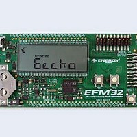
EFM32-TG-STK3300
Specifications of EFM32-TG-STK3300
Available stocks


Related parts for EFM32-TG-STK3300

EFM32-TG-STK3300 Summary of contents
Page 1
... The EFM32 microcontroller family revolutionizes the 8- to 32-bit market with a combination of unmatched performance and ultra low power consumption in both active- and sleep modes. EFM32 devices only consume 180 µA per MHz in run mode. EFM32's low energy consumption by far outperforms any other available 8-, 16-, and 32-bit solution ...
Page 2
... Introduction 1.1 About this document This document provides the information required to use the ARM Cortex-M3 core in EFM32 microcontrollers. Further details on the specific implementations within the EFM32 devices can be found in the reference manual and datasheet for the specific device. This document does not provide information on debug components, features, or operation ...
Page 3
... Figure 1.1. EFM32 Cortex-M3 implementation EFM32 Cortex-M3 processor WIC NVIC Debug Access Port Code interface The Cortex-M3 processor is built on a high-performance processor core, with a 3-stage pipeline Harvard architecture, making it ideal for demanding embedded applications. The processor delivers exceptional power efficiency through an efficient instruction set and extensively optimized design, providing high- end processing hardware including single-cycle 32x32 multiplication and dedicated hardware division ...
Page 4
... The Embedded Trace Macrocell™ (ETM) delivers unrivalled instruction trace capture in an area far smaller than traditional trace units. The ETM is only available in some EFM32 devices (Table 1.1 ( 1.2.3 Cortex-M3 processor features and benefits summary • ...
Page 5
... EFM32 Cortex-M3 configurations The different EFM32 series contain different subsets of peripherals within the ARM Cortex-M3. Table 1.1 (p. 5) shows which features are included in the different EFM32 series. Table 1.1. Cortex-M3 configuration in EFM32 series Feature ARM Cortex-M3 version and revision Number of interrupts ...
Page 6
The Cortex-M3 Processor 2.1 Programmers model This section describes the Cortex-M3 programmers model. In addition to the individual core register descriptions, it contains information about the processor modes and privilege levels for software execution and stacks. 2.1.1 Processor mode ...
Page 7
Processor Used to execute mode Handler Exception handlers 1 See Section 2.1.3.7 (p. 12) . 2.1.3 Core registers The processor core registers are: Low registers High registers R10 R11 R12 Stack Pointer SP (R13) Link Register LR (R14) Program Counter ...
Page 8
Name Type Required 2 privilege PRIMASK RW Privileged FAULTMASK RW Privileged BASEPRI RW Privileged CONTROL RW Privileged 1 Describes access type during program execution in thread mode and Handler mode. Debug access can differ entry of Either ...
Page 9
ICI/IT T Access these registers individually combination of any two or all three registers, using the register name as an argument to the ...
Page 10
Interrupt Program Status Register The IPSR contains the exception type number of the current Interrupt Service Routine (ISR). See the register summary in Table 2.2 (p. 7) for its attributes. The bit assignments are: Table 2.5. IPSR bit assignments ...
Page 11
EPSR value in the stacked PSR to indicate the operation that is at fault. See Section 2.3.7 (p. 26) 2.1.3.5.4 Interruptible-continuable instructions When an interrupt occurs during the execution of an LDM or STM instruction, the processor: ...
Page 12
Table 2.8. FAULTMASK register bit assignments Bits Name Function [31:1] - Reserved [0] FAULTMASK effect 1 = prevents the activation of all exceptions except for NMI. The processor clears the FAULTMASK bit exit ...
Page 13
Table 2.10. CONTROL register bit assignments Bits Name [31:2] - [1] Active stack pointer [0] Thread mode privilege level Handler mode always uses the MSP, so the processor ignores explicit writes to the active stack pointer bit of the CONTROL ...
Page 14
RTOS kernels, including a debug channel. The CMSIS includes address definitions ...
Page 15
Bit band region 0x40000000 0x23FFFFFF 32MB 0x22000000 0x200FFFFF 1MB Bit band region 0x20000000 The regions for SRAM and peripherals include bit-band regions. Bit-banding provides atomic operations to bit data, see Section 2.2.5 (p. 18) . ...
Page 16
Device The processor preserves transaction order relative to other transactions to Device or Strongly-ordered memory. Strongly-ordered The processor preserves transaction order relative to all other transactions. The different ordering requirements for Device and Strongly-ordered memory mean that the memory system ...
Page 17
Address Memory region Memory range type External RAM Normal 0x60000000- 0x9FFFFFFF External device Device 0xA0000000- 0xDFFFFFFF Private Strongly- 0xE0000000- Peripheral Bus ordered 0xE00FFFFF Reserved Device 0xE0100000- 0xFFFFFFFF 1 See Section 2.2.1 (p. 15) for more information. The Code, SRAM, and ...
Page 18
Self-modifying code program contains self-modifying code, use an ISB instruction immediately after the code modification in the program. This ensures subsequent instruction execution uses the updated program. • Memory map switching. If the system contains a memory ...
Page 19
Bit_word_offset is the position of the target bit in the bit-band memory region. • Bit_word_addr is the address of the word in the alias ...
Page 20
... Section 2.2.6.1 (p. 20) describes how words of data are stored in memory. 2.2.6.1 Little-endian format The EFM32 uses a little-endian format, in which the processor stores the least significant byte of a word at the lowest-numbered byte, and the most significant byte at the highest-numbered byte. For example: ...
Page 21
LDREX and STREX • the halfword instructions LDREXH and STREXH • the byte instructions LDREXB and STREXB. Software must use a Load-Exclusive instruction with the corresponding Store-Exclusive instruction. To perform a guaranteed read-modify-write of a memory ...
Page 22
... When reset is deasserted, execution restarts from the address provided by the reset entry in the vector table. Execution restarts as privileged execution in Thread mode. In the EFM32 devices a NonMaskable Interrupt (NMI) can only be triggered by software. This is the highest priority exception other than reset permanently enabled and has a fixed priority of -2. NMIs cannot be: • ...
Page 23
Usage fault SVCall PendSV SysTick Interrupt (IRQ) Table 2.15. Properties of the different exception types Exception IRQ Exception type 1 1 number number 1 - Reset 2 -14 NMI 3 -13 Hard fault 4 -12 Memory management fault 5 -11 ...
Page 24
Privileged software can disable the exceptions that Table 2.15 (p. 23) shows as having configurable priority, see: • Section 4.3.10 (p. 103) • Section 4.2.3 (p. 90) . For more information about hard faults, memory management faults, bus faults, and ...
Page 25
Figure 2.2. Vector table Exception num ber IRQ num ber n+ 16 n-1 0x040+ 4x(n- -10 5 -11 ...
Page 26
For example, assigning a higher priority value to IRQ[0] and a lower priority value to IRQ[1] means that IRQ[1] has higher priority than IRQ[0]. If both IRQ[1] and IRQ[0] are asserted, IRQ[1] is processed before IRQ[0]. If multiple pending exceptions ...
Page 27
On return from the exception handler of the late-arriving exception, the normal tail-chaining rules apply. 2.3.7.1 Exception entry Exception entry occurs when there is a pending exception with sufficient priority and either: ...
Page 28
Table 2.16 (p. 28) shows the EXC_RETURN[3:0] values with a description of the exception return behavior. The processor sets EXC_RETURN bits[31:4] to 0xFFFFFFF. When this value is loaded into ...
Page 29
Fault during exception stacking during exception unstacking Bus error: during exception stacking during exception unstacking during instruction prefetch Precise data bus error Imprecise data bus error Attempt to access a coprocessor Undefined instruction Attempt to enter an invalid instruction set ...
Page 30
Table 2.18. Fault status and fault address registers Handler Status register name Hard fault HFSR Memory management MMFSR fault Bus fault BFSR Usage fault UFSR 2.4.4 Lockup The processor enters a lockup state if a hard fault occurs when executing ...
Page 31
See Section 3.10.11 (p. ...
Page 32
If the processor detects a connection to a debugger it disables the WIC. 2.5.4 Power management programming hints ANSI C cannot directly generate the WFI and WFE instructions. The CMSIS provides the following intrinsic functions for these instructions: void __WFE(void) ...
Page 33
The Cortex-M3 Instruction Set 3.1 Instruction set summary The processor implements a version of the Thumb instruction set. Table 3.1 (p. 33) lists the supported instructions. Note In Table 3.1 (p. 33) : • angle brackets, <>, enclose alternative ...
Page 34
Mnemonic Operands - CLREX CLZ Rd, Rm CMN, CMNS Rn, Op2 CMP, CMPS Rn, Op2 CPSID iflags CPSIE iflags DMB - DSB - EOR, EORS {Rd,} Rn, Op2 ISB - - IT LDM Rn{!}, reglist LDMDB, Rn{!}, reglist LDMEA LDMFD, ...
Page 35
Mnemonic Operands MLA Rd, Rn, Rm, Ra MLS Rd, Rn, Rm, Ra MOV, MOVS Rd, Op2 MOVT Rd, #imm16 MOVW, MOV Rd, #imm16 MRS Rd, spec_reg MSR spec_reg, Rm MUL, MULS {Rd,} Rn, Rm MVN, MVNS Rd, Op2 - NOP ...
Page 36
Mnemonic Operands RdLo, RdHi, Rn, Rm Signed Multiply (32 x 32), 64-bit result SMULL SSAT Rd, #n, Rm {,shift #s} STM Rn{!}, reglist STMDB, Rn{!}, reglist STMEA STMFD, Rn{!}, reglist STMIA STR Rt, [Rn, #offset] STRB, STRBT Rt, [Rn, #offset] ...
Page 37
Mnemonic Operands USAT Rd, #n, Rm {,shift #s} {Rd,} Rm {,ROR #n} Zero extend a byte UXTB {Rd,} Rm {,ROR #n} Zero extend a halfword UXTH - WFE - WFI 3.2 Intrinsic functions ANSI cannot directly access some Cortex-M3 instructions. ...
Page 38
Special register Access CMSIS function Write void __set_PRIMASK (uint32_t value) FAULTMASK Read uint32_t __get_FAULTMASK (void) Write void __set_FAULTMASK (uint32_t value) BASEPRI Read uint32_t __get_BASEPRI (void) Write void __set_BASEPRI (uint32_t value) CONTROL Read uint32_t __get_CONTROL (void) Write void __set_CONTROL (uint32_t value) ...
Page 39
#constant where constant can be: • any constant that can be produced by shifting an 8#bit value left by any number of bits within a 32#bit word • any constant of the form 0x00XY00XY • any constant of the form ...
Page 40
ASR, LSR, LSL, ROR, and RRX, and the result is written to a destination register • during the calculation of Operand2 by the instructions that specify the second operand as a register with shift, see ...
Page 41
Figure 3.2. LSR # 3.3.4.3 LSL Logical shift left by n bits moves the right-hand 32-n bits of the register Rm, to the left by n places, into the left-hand 32-n bits of the result. And ...
Page 42
Figure 3.4. ROR #3 31 3.3.4.5 RRX Rotate right with extend moves the bits of the register Rm to the right by one bit. And it copies the carry flag into bit[31] of the result. See Figure 3.5 (p. 42) ...
Page 43
Note • For B, BL, CBNZ, and CBZ instructions, the value of the PC is the address of the current instruction plus 4 bytes. • For all other instructions that use labels, the value of the PC is the address ...
Page 44
• if the result of an addition is greater than or equal to 2 • if the result of a subtraction is positive or zero • as the result of an inline barrel shifter operation in a move or logical ...
Page 45
Example 3.2 (p. 45) shows the use of conditional instructions to update the value the signed values R0 is greater than R1 and R2 is greater than R3. Example 3.2. Compare and update value CMP R0, R1 ...
Page 46
Mnemonic Brief description Store Register using register offset STR{type} Store Register with unprivileged access STR{type}T STREX{type} Store Register Exclusive 3.4.1 ADR Load PC-relative address. 3.4.1.1 Syntax ADR{cond} Rd, label where optional condition code, see Section 3.3.7 (p. 43) ...
Page 47
Rt, [Rn, #offset]! op{type}{cond} Rt, [Rn], #offset opD{cond} Rt, Rt2, [Rn {, #offset}] opD{cond} Rt, Rt2, [Rn, #offset]! opD{cond} Rt, Rt2, [Rn], #offset where: is one of: op LDR Load Register. STR Store Register. is one of: type unsigned ...
Page 48
The value to load or store can be a byte, halfword, word, or two words. Bytes and halfwords can either be signed or unsigned. See Section 3.3.5 (p. 42) . Table 3.6 (p. 48) shows the ranges of offset for ...
Page 49
Syntax op{type}{cond} Rt, [Rn LSL #n}] where: is one of: op LDR Load Register. STR Store Register. is one of: type unsigned byte, zero extend to 32 bits on loads signed byte, sign extend to ...
Page 50
LDRSB R0, [R5, R1, LSL #1] ; Read byte value from an address equal to STR R0, [R1, R2, LSL #2] ; Stores address equal to sum of R1 3.4.4 LDR and STR, unprivileged Load and Store ...
Page 51
LDR, PC#relative Load register from memory. 3.4.5.1 Syntax LDR{type}{cond} Rt, label LDRD{cond} Rt, Rt2, label where: is one of: type unsigned byte, zero extend to 32 bits signed byte, sign extend to 32 bits. unsigned halfword, zero ...
Page 52
IT block. 3.4.5.4 Condition flags These instructions do not change the flags. 3.4.5.5 Examples LDR R0, LookUpTable LDRSB R7, localdata 3.4.6 LDM and STM Load and ...
Page 53
If the writeback suffix is specified, the value (n-1) is written back to Rn. For LDMDB, LDMEA, STMDB, and STMFD the ...
Page 54
PUSH and POP are synonyms for STMDB and LDM (or LDMIA) with the memory addresses for the access based on SP, and with the final address for the access written back to the SP. PUSH and POP are the preferred ...
Page 55
STREXH{cond} Rd, Rt, [Rn] where optional condition code, see Section 3.3.7 (p. 43) . cond is the destination register for the returned status the register to load or store the register on which the ...
Page 56
CLREX Clear Exclusive. 3.4.9.1 Syntax CLREX{cond} where: cond is an optional condition code, see Section 3.3.7 (p. 43) . 3.4.9.2 Operation Use CLREX to make the next STREX, STREXB, or STREXH instruction write 1 to its destination register and ...
Page 57
Mnemonic Brief description Move NOT MVN Logical OR NOT ORN Logical OR ORR Reverse Bits RBIT Reverse byte order in a word REV Reverse byte order in each halfword REV16 Reverse byte order in bottom halfword and sign extend REVSH ...
Page 58
The SBC instruction subtracts the value of Operand2 from the value in Rn. If the carry flag is clear, the result is reduced by one. The RSB instruction subtracts the value in Rn from the value of Operand2. This is ...
Page 59
Multiword arithmetic examples Example 3.4 (p. 59) shows two instructions that add a 64#bit integer contained in R2 and R3 to another 64#bit integer contained in R0 and R1, and place the result in R4 and R5. Example 3.4. ...
Page 60
Condition flags specified, these instructions: • update the N and Z flags according to the result • can update the C flag during the calculation of Operand2, see Section 3.3.3 (p. 38) • do not affect ...
Page 61
RRX moves the bits in register Rm to the right all these instructions, the result is written to Rd, but the value in register Rm remains unchanged. For details on what result is generated by the different ...
Page 62
CMP and CMN Compare and Compare Negative. 3.5.5.1 Syntax CMP{cond} Rn, Operand2 CMN{cond} Rn, Operand2 where optional condition code, see Section 3.3.7 (p. 43) . cond is the register holding the first operand. Rn Operand2 is a ...
Page 63
specified, the condition code flags are updated on the result of S the operation, see Section 3.3.7 (p. 43 optional condition code, see Section 3.3.7 (p. 43) . cond ...
Page 64
N and Z flags according to the result • can update the C flag during the calculation of Operand2, see Section 3.3.3 (p. 38) • do not affect the V flag. 3.5.6.5 Example MOVS R11, #0x000B ; ...
Page 65
Reverse byte order in a word. REV REV16 Reverse byte order in each halfword independently. REVSH Reverse byte order in the bottom halfword, and sign extend to 32 bits. Reverse the bit order in a ...
Page 66
Operation These instructions test the value in a register against Operand2. They update the condition flags based on the result, but do not write the result to a register. The TST instruction performs a bitwise AND operation on the ...
Page 67
Mnemonic Brief description Unsigned Multiply (32x32), 64-bit result UMULL 3.6.1 MUL, MLA, and MLS Multiply, Multiply with Accumulate, and Multiply with Subtract, using 32#bit operands, and producing a 32-bit result. 3.6.1.1 Syntax MUL{S}{cond} {Rd,} Rn Multiply MLA{cond} Rd, ...
Page 68
Examples MUL R10, R2, R5 MLA R10, R2, R1 Multiply with accumulate, R10 = ( MULS R0, R2, R2 MULLT R2, R3, R2 MLS R4, R5, R6, R7 3.6.2 UMULL, UMLAL, SMULL, and ...
Page 69
Examples UMULL R0, R4, R5, R6 SMLAL R4, R5, R3, R8 3.6.3 SDIV and UDIV Signed Divide and Unsigned Divide. 3.6.3.1 Syntax SDIV{cond} {Rd,} Rn, Rm UDIV{cond} {Rd,} Rn, Rm where: cond is an optional condition code, see Section ...
Page 70
shift#s 3.7.1.2 Operation These instructions saturate to a signed or unsigned n-bit value. The SSAT instruction applies the specified shift, then saturates to the signed range #2 The USAT instruction applies the specified shift, ...
Page 71
USATNE R0, #7, R5 3.8 Bitfield instructions Table 3.10 (p. 71) shows the instructions that operate on adjacent sets of bits in registers or bitfields: Table 3.10. Packing and unpacking instructions Mnemonic Brief description Bit Field Clear BFC Bit Field ...
Page 72
Examples BFC R4, #8, #12 BFI R9, R2, #8, #12 3.8.2 SBFX and UBFX Signed Bit Field Extract and Unsigned Bit Field Extract. 3.8.2.1 Syntax SBFX{cond} Rd, Rn, #lsb, #width UBFX{cond} Rd, Rn, #lsb, #width where optional ...
Page 73
UXTextend{cond} {Rd ROR #n} where: extend is one of: B Extends an 8#bit value to a 32#bit value. H Extends a 16#bit value to a 32#bit value optional condition code, see Section 3.3.7 (p. 43) . ...
Page 74
Mnemonic Brief description Branch indirect BX Compare and Branch if Non Zero CBNZ Compare and Branch if Non Zero CBZ If#Then IT Table Branch Byte TBB Table Branch Halfword TBH 3.9.1 B, BL, BX, and BLX Branch instructions. 3.9.1.1 Syntax ...
Page 75
Instruction Branch range Bcond label (inside IT block) # + +16 MB BL{cond} label Any value in register BX{cond} Rm Any value in register BLX{cond} Rm Note You might have to use the .W ...
Page 76
Operation Use the CBZ or CBNZ instructions to avoid changing the condition code flags and to reduce the number of instructions. CBZ Rn, label does not change condition flags but is otherwise equivalent to: CMP Rn, #0 BEQ label ...
Page 77
Operation The IT instruction makes up to four following instructions conditional. The conditions can be all the same, or some of them can be the logical inverse of the others. The conditional instructions following the IT instruction form the ...
Page 78
ITTE NE ; Next 3 instructions are conditional ANDNE R0, R0 ANDNE does not update condition flags ADDSNE R2, R2 ADDSNE updates condition flags MOVEQ R2 Conditional move CMP R0 Convert R0 ...
Page 79
Rm must not be SP and must not be PC • when any of these instructions is used inside an IT block, it must be the last instruction of the IT block. 3.9.4.4 Condition flags These instructions do not ...
Page 80
Mnemonic Brief description Move from special register to register MRS Move from register to special register MSR No Operation NOP Send Event SEV Supervisor Call SVC Wait For Event WFE Wait For Interrupt WFI 3.10.1 BKPT Breakpoint. 3.10.1.1 Syntax BKPT ...
Page 81
CPSeffect iflags where: effect is one of: IE Clears the special purpose register. ID Sets the special purpose register. iflags is a sequence of one or more flags: i Set or clear PRIMASK. f Set or clear FAULTMASK. 3.10.2.2 Operation ...
Page 82
Examples DMB ; Data Memory Barrier 3.10.4 DSB Data Synchronization Barrier. 3.10.4.1 Syntax DSB{cond} where: cond is an optional condition code, see Section 3.3.7 (p. 43) . 3.10.4.2 Operation DSB acts as a special data synchronization memory barrier. Instructions ...
Page 83
ISB ; Instruction Synchronisation Barrier 3.10.6 MRS Move the contents of a special register to a general#purpose register. 3.10.6.1 Syntax MRS{cond} Rd, spec_reg where optional condition code, see Section 3.3.7 (p. 43) . cond is the destination register. ...
Page 84
Rn spec_reg can be any of: APSR, IPSR, EPSR, IEPSR, IAPSR, EAPSR, PSR, MSP, PSP, PRIMASK, BASEPRI, BASEPRI_MAX, FAULTMASK, or CONTROL. 3.10.7.2 Operation The register access operation in MSR depends on the privilege level. Unprivileged software ...
Page 85
NOP ; No operation 3.10.9 SEV Send Event. 3.10.9.1 Syntax SEV{cond} where: cond is an optional condition code, see Section 3.3.7 (p. 43) . 3.10.9.2 Operation SEV is a hint instruction that causes an event to be signaled to all ...
Page 86
PC) 3.10.11 WFE Wait For Event. 3.10.11.1 Syntax WFE{cond} where: cond is an optional condition code, see Section 3.3.7 (p. 43) . 3.10.11.2 Operation WFE is a hint instruction. If the event register ...
Page 87
Debug Entry request, regardless of whether Debug is enabled. 3.10.12.3 Condition flags This instruction does not change the flags. 3.10.12.4 Examples WFI ; Wait for interrupt 2011-02-04 - d0002_Rev1.00 ...the world's most energy friendly microcontrollers www.energymicro.com 87 ...
Page 88
The Cortex-M3 Peripherals 4.1 About the peripherals The address map of the Private peripheral bus (PPB) is: Table 4.1. Core peripheral register regions Address Core peripheral System control block 0xE000E008-0xE000E00F System timer 0xE000E010-0xE000E01F Nested Vectored Interrupt Controller 0xE000E100-0xE000E4EF System ...
Page 89
Address Name Type ISPR0- RW 0XE000E200- ISPR1 0XE000E204 ICPR0- RW 0XE000E280- ICPR1 0XE000E284 IABR0- RO 0xE000E300- IABR1 0xE000E304 IPR0- RW 0xE000E400- IPRm 0xE000E400+4xm STIR WO 0xE000EF00 1 m=(n-1)/4, where n denotes the number of interrupts given in Table 1.1 (p. ...
Page 90
Table 4.4. ISER bit assignments Bits Name Function [31:0] SETENA Interrupt set-enable bits. Write effect1 = enable interrupt.Read interrupt disabled 1 = interrupt enabled pending interrupt is enabled, the NVIC activates the interrupt ...
Page 91
Table 4.6. ISPR bit assignments Bits Name Function [31:0] SETPEND Interrupt set-pending bits. Write effect 1 = changes interrupt state to pending.Read interrupt is not pending 1 = interrupt is pending. Note Writing 1 to ...
Page 92
Table 4.8. IABR bit assignments Bits Name Function [31:0] ACTIVE Interrupt active flags interrupt not active 1 = interrupt active. A bit reads as one if the status of the corresponding interrupt is active or active and ...
Page 93
... Table 1.1 ( For example, a value of b000000011 specifies interrupt IRQ3. 4.2.9 Level-sensitive interrupts All interrupt lines in the EFM32 devices are level sensitive interrupts. A level-sensitive interrupt is held asserted until the peripheral deasserts the interrupt signal. Typically this happens because the ISR accesses the peripheral, causing it to clear the interrupt request. ...
Page 94
If the interrupt signal is still asserted, the state of the interrupt does not change. Otherwise, the state of the interrupt changes to inactive. 4.2.10 NVIC design hints and tips Ensure software uses correctly aligned register accesses. The processor does ...
Page 95
Address Name Type Required privilege 0xE000ED00 CPUID RO Privileged 1 0xE000ED04 ICSR RW Privileged 0xE000ED08 VTOR RW Privileged 1 0xE000ED0C AIRCR RW Privileged 0xE000ED10 SCR RW Privileged 0xE000ED14 CCR RW Privileged 0xE000ED18 SHPR1 RW Privileged 0xE000ED1C SHPR2 RW Privileged 0xE000ED20 ...
Page 96
Bits Name Function [2] DISFOLD When set to 1, disables IT folding. see Section 4.3.2.1 (p. 96) for more information. [1] DISDEFWBUF When set to 1, disables write buffer use during default memory map accesses. This causes all bus faults ...
Page 97
See the register summary in Table 4.12 (p. 94) , and the Type descriptions in Table 4.15 (p. 97) , for the ICSR attributes. The bit assignments are Table ...
Page 98
Bits Name Type [25] PENDSTCLR WO [24 [23] Reserved for RO Debug use [22] ISRPENDING RO [21:18 [17:12] VECTPENDING RO [11] RETTOBASE RO [10: [8:0] VECTACTIVE RO 1 This is the same value ...
Page 99
... Reserved. When setting TBLOFF, you must align the offset to the number of exception entries in the vector table. The recommended alignment is 64 words, which covers all EFM32 interrupts and the 16 internal Cortex- M3 exceptions. If you require 16 interrupts or less, the alignment can be set to 32 words. ...
Page 100
... Function System reset request system reset request 1 = asserts a signal to the EFM32 Reset Managment Unit (RMU) to request a reset. This is intended to force a large system reset of all major components except for debug. This bit reads as 0. ...
Page 101
Bits Name Function [4] SEVONPEND Send Event on Pending bit only enabled interrupts or events can wakeup the processor, disabled interrupts are excluded1 = enabled events and all interrupts, including disabled interrupts, can wakeup the processor. When an ...
Page 102
Bits Name [8] BFHFNMIGN [7:5] - [4] DIV_0_TRP [3] UNALIGN_TRP [2] - [1] USERSETMPEND [0] NONEBASETHRDENA 4.3.9 System Handler Priority Registers The SHPR1-SHPR3 registers set the priority level the exception handlers that have configurable priority. SHPR1-SHPR3 ...
Page 103
... Handler Field SysTick PRI_15 Each PRI_N field is 8 bits wide, but the EFM32 implements only bits[7:5] of each field, and bits[4:0] read as zero and ignore writes. 4.3.9.1 System Handler Priority Register 1 The bit assignments are Reserved Table 4.22. SHPR1 register bit assignments ...
Page 104
SVC exceptions • the active status of the system handlers. See the register summary in Table 4.12 (p. 94) for the SHCSR attributes. The bit assignments are: 31 ...
Page 105
Active bits, read the exception is active not active. You can write to these bits to change the active status of the exceptions, but see the Caution in this section. ...
Page 106
MMARVALID Reserved MSTKERR MUNSTKERR Reserved DACCVIOL IACCVIOL Table 4.26. MMFSR bit assignments Bits Name Function [7] MMARVALID Memory Management Fault Address Register (MMAR) valid flag value in MMAR is not ...
Page 107
Bus Fault Status Register The flags in the BFSR indicate the cause of a bus access fault. The bit assignments are BFARVALID Reserved STKERR UNSTKERR IMPRECISERR PRECISERR IBUSERR Table 4.27. BFSR ...
Page 108
Bits Name Function data bus error has occurred, and the PC value stacked for the exception return points to the instruction that caused the fault. When the processor sets this bit writes the faulting ...
Page 109
Bits Name Function When this bit is set to 1, the PC value stacked for the exception return points to the instruction that tried to perform the illegal load of the PC. [1] INVSTATE Invalid state usage fault ...
Page 110
Bits Name Function When this bit is set to 1, the PC value stacked for the exception return points to the instruction that was preempted by the exception. [0] - Reserved. Note The HFSR bits are sticky. This means as ...
Page 111
Software must follow this sequence because another higher priority exception might change the MMFAR or BFAR value. For example higher priority handler preempts the current fault handler, the other fault might change the MMFAR or BFAR value. 4.4 ...
Page 112
Bits Name Function [0] ENABLE Enables the counter counter disabled 1 = counter enabled. When ENABLE is set to 1, the counter loads the RELOAD value from the LOAD register and then counts down. On reaching 0, it ...
Page 113
SysTick Calibration Value Register The CALIB register indicates the SysTick calibration properties and is a read only register. See the register summary in Table 4.32 (p. 111) for its attributes. The bit assignments are Reserved ...
Page 114
... Table 4.37 (p. 114) shows the possible MPU region attributes. Please not that the Shareability and cache behavior attributes are usually not relevant for the EFM32 devices since these are not used by other bus masters. However, these can be useful together with the DMA Controller. See Section 4 ...
Page 115
Reserved Table 4.39. TYPE register bit assignments Bits Name Function [31:24] - Reserved. [23:16] IREGION Indicates the number of supported MPU instruction regions. Always contains 0x00. The MPU memory map is unified and is described by the ...
Page 116
Bits Name Function 0 = MPU is disabled during hard fault, NMI, and FAULTMASK handlers, regardless of the value of the ENABLE bit 1 = the MPU is enabled during hard fault, NMI, and FAULTMASK handlers. When the MPU is ...
Page 117
MPU Region Base Address Register The RBAR defines the base address of the MPU region selected by the RNR, and can update the value of the RNR. See the register summary in Table 4.38 (p. 114) for its attributes. ...
Page 118
RASR is accessible using word or halfword accesses: • the most significant halfword holds the region attributes • the least significant halfword holds the region size and the region and subregion enable bits. The bit assignments are ...
Page 119
SIZE value Region size Value of N b01001 (9) 1KB 10 b10011 (19) 1MB 20 b11101 (29) 1GB 30 b11111 (31) 4GB b01100 1 In the RBAR, see Section 4.5.4 (p. 117) . 4.5.6 MPU access permission attributes This section ...
Page 120
Table 4.47 (p. 120) shows the AP encodings that define the access permissions for privileged and unprivileged software. Table 4.47. AP encoding AP[2:0] Privileged Unprivileged permissions permissions 000 No access No access 001 RW No access 010 RW RO 011 ...
Page 121
R1 = region number ; R2 = size/enable ; R3 = attributes ; R4 = address LDR R0,=MPU_RNR ; 0xE000ED98, MPU region number register STR R1, [R0, #0x0] ; Region Number BIC R2, R2 Disable STRH R2, ...
Page 122
R3 = size, attributes in one LDR R0, =MPU_RNR ; 0xE000ED98, MPU region number register STR R1, [R0, #0x0] ; Region Number STR R2, [R0, #0x4] ; Region Base Address STR R3, [R0, #0x8] ; Region Attribute, Size and ...
Page 123
... In the EFM32 devices the shareability and cache policy attributes do not affect the system behavior. However, using these settings for the MPU regions can make the application code more portable and also be useful for setups with the DMA Controller. The values given are for typical situations. ...
Page 124
Glossary This glossary describes some of the terms used in technical documents from ARM. Abort A mechanism that indicates to a processor that the value associated with a memory access is invalid. An abort can be caused by the external ...
Page 125
Condition field A four-bit field in an instruction that specifies a condition under which the instruction can execute. Conditional execution If the condition code flags indicate that the ...
Page 126
Implementation-specific The behavior is not architecturally defined, and does not have to be documented by individual implementations. Used when there are a number of implementation options available and the option chosen does not affect software compatibility. Index register In some ...
Page 127
Should Be Zero (SBZ) Write all 0s for bit fields, by software. Writing as 1 produces Unpredictable results. Should Be Zero or Write all 0s for bit fields, by software, or preserved by writing ...
Page 128
... Revision History 5.1 Revision 1.00 February 4th, 2011 Updated document to reflect all EFM32 ARM Cortex-M3 devices. Added information on differences between EFM32G, EFM32GG and EFM32TG devices. 5.2 Revision 0.81 December 9th, 2009 Corrected intrinsic function for Wait For Interrupt in 2.5.4 Added description of all PRIGROUP settings in Table 4-18 5 ...
Page 129
... A.2 Trademark Information Energy Micro, EFM32, EFR, logo and combinations thereof, and others are the registered trademarks or trademarks of Energy Micro AS. ARM, CORTEX, THUMB are the registered trademarks of ARM Limited. Other terms and product names may be trademarks of others. ...
Page 130
... B Contact Information B.1 Energy Micro Corporate Headquarters Postal Address Energy Micro AS P.O. Box 4633 Nydalen N-0405 Oslo NORWAY www.energymicro.com Phone: + Fax B.2 Global Contacts Visit www.energymicro.com for information on global distributors and representatives or contact sales@energymicro.com for additional information. Americas www.energymicro.com/americas www.energymicro.com/emea 2011-02-04 - d0002_Rev1.00 ...
Page 131
... Table of Contents 1. Introduction .............................................................................................................................................. 2 1.1. About this document ....................................................................................................................... 2 1.2. About the EFM32 Cortex-M3 processor and core peripherals .................................................................. 2 2. The Cortex-M3 Processor ........................................................................................................................... 6 2.1. Programmers model ........................................................................................................................ 6 2.2. Memory model .............................................................................................................................. 14 2.3. Exception model ........................................................................................................................... 22 2.4. Fault handling .............................................................................................................................. 28 2.5. Power management ....................................................................................................................... 30 3. The Cortex-M3 Instruction Set ................................................................................................................... 33 3.1. Instruction set summary ................................................................................................................. 33 3 ...
Page 132
... List of Figures 1.1. EFM32 Cortex-M3 implementation ............................................................................................................. 3 2.1. Bit-band mapping ................................................................................................................................. 19 2.2. Vector table ......................................................................................................................................... 25 3.1. ASR #3 ............................................................................................................................................... 40 3.2. LSR #3 ............................................................................................................................................... 41 3.3. LSL #3 ................................................................................................................................................ 41 3.4. ROR #3 .............................................................................................................................................. 42 3.5. RRX ................................................................................................................................................... 42 2011-02-04 - d0002_Rev1.00 ...the world's most energy friendly microcontrollers www.energymicro.com 132 ...
Page 133
... List of Tables 1.1. Cortex-M3 configuration in EFM32 series .................................................................................................... 5 2.1. Summary of processor mode, execution privilege level, and stack use options .................................................... 6 2.2. Core register set summary ....................................................................................................................... 7 2.3. PSR register combinations ....................................................................................................................... 9 2.4. APSR bit assignments ............................................................................................................................. 9 2.5. IPSR bit assignments ............................................................................................................................ 10 2.6. EPSR bit assignments ........................................................................................................................... 10 2.7. PRIMASK register bit assignments ........................................................................................................... 11 2 ...
Page 134
MPU CTRL register bit assignments ...................................................................................................... 115 4.41. RNR bit assignments .......................................................................................................................... 116 4.42. RBAR bit assignments ........................................................................................................................ 117 4.43. RASR bit assignments ........................................................................................................................ 118 4.44. Example SIZE field values ................................................................................................................... 118 4.45. TEX and S encoding ...
Page 135
List of Examples 3.1. Absolute value ...................................................................................................................................... 44 3.2. Compare and update value ..................................................................................................................... 45 3.3. Instruction width selection ....................................................................................................................... 45 3.4. 64-bit addition ...................................................................................................................................... 59 3.5. 96-bit subtraction .................................................................................................................................. 59 2011-02-04 - d0002_Rev1.00 ...the world's most energy friendly microcontrollers ...
Page 136
...