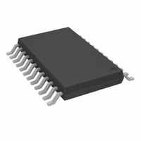
AD7190BRUZ-REEL Analog Devices Inc, AD7190BRUZ-REEL Datasheet - Page 25

AD7190BRUZ-REEL
Manufacturer Part Number
AD7190BRUZ-REEL
Description
2ch UltraLow Noise 24Bit SD ADC IC.
Manufacturer
Analog Devices Inc
Datasheet
1.AD7190BRUZ.pdf
(40 pages)
Specifications of AD7190BRUZ-REEL
Design Resources
Precision Weigh Scale Design Using AD7190 with Internal PGA (CN0102)
Number Of Bits
24
Sampling Rate (per Second)
4.8k
Data Interface
DSP, MICROWIRE™, QSPI™, Serial, SPI™
Number Of Converters
1
Voltage Supply Source
Analog and Digital
Operating Temperature
-40°C ~ 105°C
Mounting Type
Surface Mount
Package / Case
24-TSSOP (0.173", 4.40mm Width)
Lead Free Status / RoHS Status
Lead free / RoHS Compliant
Available stocks
Company
Part Number
Manufacturer
Quantity
Price
Company:
Part Number:
AD7190BRUZ-REEL
Manufacturer:
ADI
Quantity:
1 000
Part Number:
AD7190BRUZ-REEL
Manufacturer:
ADI/亚德诺
Quantity:
20 000
GP7
0(0)
Table 21. Register Bit Designations
Bit Location
GP7
GP 6
GP5
GP4
GP3
GP2
GP1
GP0
OFFSET REGISTER
(RS2, RS1, RS0 = 1, 1, 0; Power-On/Reset = 0x800000)
The offset register holds the offset calibration coefficient for the
ADC. The power-on reset value of the offset register is 0x800000.
The AD7190 has four offset registers; therefore, each channel
has a dedicated offset register. Each of these registers is a 24-bit
read/write register. This register is used in conjunction with its
associated full-scale register to form a register pair. The power-
on reset value is automatically overwritten if an internal or
system zero-scale calibration is initiated by the user. The AD7190
must be placed in power-down mode or idle mode when writing
to the offset register.
GP6
BPDSW(0)
0
P3DAT
P2DAT
P1DAT
P0DAT
Bit Name
BPDSW
GP32EN
GP10EN
GP5
GP32EN(0)
Description
This bit must be programmed with a Logic 0 for correct operation.
Bridge power-down switch control bit. This bit is s
BPDSW to AGND. The switch can sink up to 30 mA. The bit is cleared by the user to open the bridge power-
down switch. When the ADC is placed in power-down mode, the bridge power-down switch remains active.
Digital Output P3 and Digital Output P2 enable. When GP32EN is set, the digital outputs, P3 and P2, are
active. When GP32EN is cleared, the P3 and P2 pins are tristated, and the P3DAT and P2DAT bits are ignored.
Digital Output P1 and Digital Output P0 enable. When GP10EN is set, the digital outputs, P1 and P0, are
active. When GP10EN is cleared, the P1 and P0 outputs are tristated, and the P1DAT and P0DAT bits are
ignored. The P1 and P0 pins can be used as a reference input REFIN2 when the REFSEL bit in the
configuration register is set to 1.
Digital Output P3. When GP32EN is set, the P3DAT bit sets the value of the P3 general-purpose output pin.
When P3DAT is high, the P3 output pin is high. When P3DAT is low, the P3 output pin is low. When the
GPOCON register is read, the P3DAT bit reflects the status of the P3 pin if GP32EN is set.
Digital Output P2. When GP32EN is set, the P2DAT bit sets the value of the P2 general-purpose output pin.
When P2DAT is high, the P2 output pin is high. When P2DAT is low, the P2 output pin is low. When the
GPOCON register is read, the P2DAT bit reflects the status of the P2 pin if GP32EN is set.
Digital Output P1. When GP10EN is set, the P1DAT bit sets the value of the P1 general-purpose output pin.
When P1DAT is high, the P1 output pin is high. When P1DAT is low, the P1 output pin is low. When the
GPOCON register is read, the P1DAT bit reflects the status of the P1 pin if GP10EN is set.
Digital Output P0. When GP10EN is set, the P0DAT bit sets the value of the P0 general-purpose output pin.
When P0DAT is high, the P0 output pin is high. When P0DAT is low, the P0 output pin is low. When the
GPOCON register is read, the P0DAT bit reflects the status of the P0 pin if GP10EN is set.
GP4
GP10EN(0)
Rev. B | Page 25 of 40
GP3
P3DAT(0)
FULL-SCALE REGISTER
(RS2, RS1, RS0 = 1, 1, 1; Power-On/Reset = 0x5XXXX0)
The full-scale register is a 24-bit register that holds the full-scale
calibration coefficient for the ADC. The AD7190 has four full-
scale registers; therefore, each channel has a dedicated full-scale
register. The full-scale registers are read/write registers. However,
when writing to the full-scale registers, the ADC must be placed
in power-down mode or idle mode. These registers are configured
at power-on with factory-calibrated, full-scale calibration coef-
ficients, the calibration being performed at gain = 1. Therefore,
every device has different default coefficients. The default value
is automatically overwritten if an internal or system full-scale
calibration is initiated by the user or if the full-scale register is
written to.
et
by the user to close the bridge power-down switch
GP2
P2DAT(0)
GP1
P1DAT(0)
GP0
P0DAT(0)
AD7190


