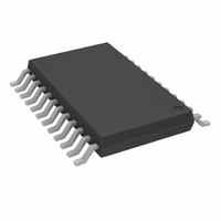
AD7190BRUZ-REEL Analog Devices Inc, AD7190BRUZ-REEL Datasheet - Page 27

AD7190BRUZ-REEL
Manufacturer Part Number
AD7190BRUZ-REEL
Description
2ch UltraLow Noise 24Bit SD ADC IC.
Manufacturer
Analog Devices Inc
Datasheet
1.AD7190BRUZ.pdf
(40 pages)
Specifications of AD7190BRUZ-REEL
Design Resources
Precision Weigh Scale Design Using AD7190 with Internal PGA (CN0102)
Number Of Bits
24
Sampling Rate (per Second)
4.8k
Data Interface
DSP, MICROWIRE™, QSPI™, Serial, SPI™
Number Of Converters
1
Voltage Supply Source
Analog and Digital
Operating Temperature
-40°C ~ 105°C
Mounting Type
Surface Mount
Package / Case
24-TSSOP (0.173", 4.40mm Width)
Lead Free Status / RoHS Status
Lead free / RoHS Compliant
Available stocks
Company
Part Number
Manufacturer
Quantity
Price
Company:
Part Number:
AD7190BRUZ-REEL
Manufacturer:
ADI
Quantity:
1 000
Part Number:
AD7190BRUZ-REEL
Manufacturer:
ADI/亚德诺
Quantity:
20 000
The sinc
120 dB, assuming a stable master clock, while the sinc
gives a rejection of 100 dB. The stop-band attenuation is
typically 53 dB for the sinc
sinc
The 3 dB frequency for the sinc
and for the sinc
Chop Enabled
With chop enabled, the ADC offset and offset drift are
minimized. When chop is enabled, the analog input pins are
continuously swapped. Therefore, with the analog input pins
connected in one direction, the settling time of the sinc filter is
allowed to elapse until a valid conversion is available. The analog
input pins are then inverted and another valid conversion is
obtained. Subsequent conversions are then averaged so that the
offset is minimized. This continuous swapping of the analog
input pins and the averaging of subsequent conversions means
that the offset drift is also minimized.
Chopping affects the output data rate and settling time of the
ADC. For the sinc
For sinc
where:
f
f
FS[9:0] is the decimal equivalent of Bit FS9 to Bit FS0 in the
mode register.
ADC
CLK
3
= master clock (4.92 MHz nominal).
is the output data rate.
f
f
f
f
filter.
3dB
3dB
ADC
ADC
–100
–10
–20
–30
–40
–50
–60
–70
–80
–90
3
0
= 0.23 × f
= 0.272 × f
Figure 20. Sinc
4
= f
= f
filter, the output data rate is equal to
0
filter provides 50 Hz (±1 Hz) rejection in excess of
CLK
CLK
/(4 × 1024 × FS[9:0])
/(3 × 1024 × FS[9:0])
3
25
filter is equal to
ADC
4
ADC
filter, the output data rate is equal to
3
Filter Response (50 Hz Output Data Rate)
50
4
FREQUENCY (Hz)
filter but equal to 40 dB for the
4
75
filter is equal to
100
125
3
filter
150
Rev. B | Page 27 of 40
The value of FS[9:0] can be varied from 1 to 1023. This results
in an output data rate of 1.173 Hz to 1200 Hz for the sinc
and 1.56 Hz to 1600 Hz for the sinc
the sinc
Therefore, with chop enabled, the settling time is reduced for a
given output data rate compared to the chop disabled mode.
However, for a given FS[9:0] value, the output data rate is less
with chop enabled compared with the chop disabled mode.
For either the sinc
equal to
Figure 21 and Figure 22 show the filter response for the sinc
and sinc
in the plots, the stop-band attenuation is less compared with the
chop disabled modes.
Figure 21. Sinc
Figure 22. Sinc
t
f
3dB
SETTLE
–100
–100
–10
–20
–30
–40
–50
–60
–70
–80
–90
–10
–20
–30
–40
–50
–60
–70
–80
–90
3
0
0
= 0.24 × f
3
or sinc
0
0
filters, respectively, when chop is enabled. As shown
= 2/f
4
3
Filter Response (Output Data Rate = 12.5 Hz, Chop Enabled)
Filter Response (Output Data Rate = 16.6 Hz, Chop Enabled)
ADC
4
25
25
filter is equal to
ADC
3
or the sinc
50
50
FREQUENCY (Hz)
FREQUENCY (Hz)
4
filter, the cutoff frequency f
75
75
3
filter. The settling time for
100
100
125
125
AD7190
150
150
4
filter
3dB
4
is


