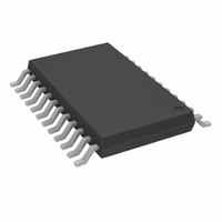
AD7190BRUZ-REEL Analog Devices Inc, AD7190BRUZ-REEL Datasheet - Page 29

AD7190BRUZ-REEL
Manufacturer Part Number
AD7190BRUZ-REEL
Description
2ch UltraLow Noise 24Bit SD ADC IC.
Manufacturer
Analog Devices Inc
Datasheet
1.AD7190BRUZ.pdf
(40 pages)
Specifications of AD7190BRUZ-REEL
Design Resources
Precision Weigh Scale Design Using AD7190 with Internal PGA (CN0102)
Number Of Bits
24
Sampling Rate (per Second)
4.8k
Data Interface
DSP, MICROWIRE™, QSPI™, Serial, SPI™
Number Of Converters
1
Voltage Supply Source
Analog and Digital
Operating Temperature
-40°C ~ 105°C
Mounting Type
Surface Mount
Package / Case
24-TSSOP (0.173", 4.40mm Width)
Lead Free Status / RoHS Status
Lead free / RoHS Compliant
Available stocks
Company
Part Number
Manufacturer
Quantity
Price
Company:
Part Number:
AD7190BRUZ-REEL
Manufacturer:
ADI
Quantity:
1 000
Part Number:
AD7190BRUZ-REEL
Manufacturer:
ADI/亚德诺
Quantity:
20 000
is 50 Hz (sinc
ADC needs to operate with an output data rate of 12.5 Hz to
obtain 50 Hz rejection when zero latency is enabled. To obtain
simultaneous 50 Hz/60 Hz rejection, the REJ60 bit in the mode
register can be set when the output data rate is equal to 12.5 Hz.
The stop-band attenuation is considerably reduced also (3 dB
compared with 53 dB in the nonzero latency mode).
Channel Sequencer
The AD7190 includes a channel sequencer, which simplifies
communications with the device in multichannel applications.
The sequencer also optimizes the channel throughput of the
device as the sequencer switches channels at the optimum rate
rather than waiting for instructions via the SPI interface.
Bits CH0 to Bit CH7 in the configuration register are used to
enable the required channels. In continuous conversion mode,
the ADC selects each of the enabled channels in sequence and
performs a conversion on the channel. The RDY pin goes low
when a valid conversion is available on each channel. When
several channels are enabled, the contents of the status register
should be attached to the 24-bit word so that the user can
identify the channel that corresponds to each conversion. To
attach the status register value to the conversion, Bit DAT_STA
in the mode register should be set to 1.
When several channels are enabled, the ADC must allow the
complete settling time to generate a valid conversion each time
that the channel is changed. The AD7190 takes care of this:
when a channel is selected, the modulator and filter are reset
and the RDY pin is taken high. The AD7190 then allows the
complete settling time to generate the first conversion.
RDY only goes low when a valid conversion is available. The
AD7190 then selects the next enabled channel and converts on
that channel. The user can then read the data register while the
ADC is performing the conversion on the next channel.
The time required to read a valid conversion from all enabled
channels is equal to
Figure 27. Sinc
t
–100
SETTLE
–10
–20
–30
–40
–50
–60
–70
–80
–90
0
0
× Number of Enabled Channels
50
4
filter); 50 Hz rejection is no longer achieved. The
4
Filter Response (50 Hz Output Data Rate, Zero Latency)
100
150
200
FREQUENCY (Hz)
250
300
350
400
450
500
550 600
Rev. B | Page 29 of 40
For example, if the sinc
zero latency is disabled, conversions are available at 1/f
converting on a single channel, where f
data rate. The settling time is equal to
The time required to sample N channels is
DIGITAL INTERFACE
As indicated in the On-Chip Registers section, the programmable
functions of the AD7190 are controlled using a set of on-chip
registers. Data is written to these registers via the serial interface
of the part. Read access to the on-chip registers is also provided
by this interface. All communication with the part must start with
a write to the communications register. After power-on or reset,
the device expects a write to its communications register. The data
written to this register determines whether the next operation is a
read operation or a write operation and also determines which
register this read or write operation affects. Therefore, write
access to any of the other registers on the part begins with a write
operation to the communications register, followed by a write to
the selected register. A read operation from any other register
(except when continuous read mode is selected) starts with a write
to the communications register, followed by a read operation from
the selected register.
The serial interface of the AD7190 consists of four signals: CS ,
DIN, SCLK, and DOUT/ RDY . The DIN line is used to transfer
data into the on-chip registers, whereas DOUT/ RDY is used for
accessing data from the on-chip registers. SCLK is the serial clock
input for the device, and all data transfers (either on DIN or
DOUT/ RDY ) occur with respect to the SCLK signal.
The DOUT/ RDY pin functions as a data ready signal also, the
line going low when a new data-word is available in the output
register. It is reset high when a read operation from the data
register is complete. It also goes high prior to the updating of the
data register to indicate when not to read from the device, to
ensure that a data read is not attempted while the register is being
updated. CS is used to select a device. It can be used to decode the
AD7190 in systems where several components are connected to
the serial bus.
CONVERSIONS
t
4/(f
SETTLE
RDY
ADC
= 4/f
× N)
CHANNEL A
ADC
Figure 28. Channel Sequencer
4
filter is selected, chop is disabled and
CHANNEL B
1/f
ADC
ADC
is equal to the output
CHANNEL C
AD7190
ADC
when


