AD9393BBCZ-80 Analog Devices Inc, AD9393BBCZ-80 Datasheet
AD9393BBCZ-80
Specifications of AD9393BBCZ-80
Available stocks


Related parts for AD9393BBCZ-80


AD9393BBCZ-80 Summary of contents
Page 1
FEATURES HDMI interface Supports high bandwidth digital content protection RGB to YCrCb 2-way color conversion 1.8 V/3.3 V power supply 76-ball BGA package RGB and YCrCb output formats Digital video interface HDMI 1.2a, DVI 1.0 80 MHz HDMI receiver Supports ...
Page 2
AD9393 TABLE OF CONTENTS Features .............................................................................................. 1 Applications ....................................................................................... 1 Functional Block Diagram .............................................................. 1 General Description ......................................................................... 1 Revision History ............................................................................... 2 Specifications ..................................................................................... 3 Electrical Characteristics ............................................................. 3 Digital Interface Electrical Characteristics ............................... 4 Absolute Maximum Ratings ............................................................ ...
Page 3
SPECIFICATIONS ELECTRICAL CHARACTERISTICS 3 1.8 V, unless otherwise noted Table 1. Parameter DIGITAL INPUTS (5 V Tolerant) Input Voltage, High ( Input Voltage, Low (V ...
Page 4
AD9393 DIGITAL INTERFACE ELECTRICAL CHARACTERISTICS =3 1.8 V, unless otherwise noted Table 2. Parameter DC DIGITAL I/O Specifications High-Level Input Voltage ( Low-Level Input Voltage (V ...
Page 5
ABSOLUTE MAXIMUM RATINGS Table 3. Parameter Digital Inputs Digital Output Current Operating Temperature Range Storage Temperature Range Maximum Junction Temperature Maximum Case Temperature Stresses above those listed under Absolute Maximum Ratings may ...
Page 6
AD9393 PIN CONFIGURATION AND FUNCTION DESCRIPTIONS 1 A D14 B D13 D11 GND K RxC– Table 4. Complete Pin List Pin No. Mnemonic Inputs B9 PD Digital Video ...
Page 7
Pin No. Mnemonic B8 VSOUT A9 O/E References D10 FILT 1 Power Supply C9, C10, D6, D7, D9, E4, GND E9, E10, F4, H10, ...
Page 8
AD9393 DESIGN GUIDE GENERAL DESCRIPTION The AD9393 is a fully integrated solution for receiving DVI/ HDMI signals and is capable of decoding HDCP-encrypted signals through connections to an external EEPROM. The circuit is ideal for providing an interface for HDTV ...
Page 9
TIMING The output data clock signal is created so that its rising edge always occurs between data transitions and can be used to latch the output data externally. Figure 3 shows the timing operation of the AD9393. t PER t ...
Page 10
AD9393 One of the three input channels is represented in Figure 4. In each processing channel, the three inputs are multiplied by three separate coefficients marked a1, a2, and a3. These coefficients are divided by 4096 to obtain nominal values ...
Page 11
AUDIO BOARD LEVEL MUTING The audio can be muted through the infoframes or locally via the serial bus registers. This can be controlled with Register 0x57, Bits[7:6]. AVI Infoframes The HDMI TMDS transmission contains infoframes with specific information for the ...
Page 12
AD9393 2-WIRE SERIAL REGISTER MAP The AD9393 is initialized and controlled by a set of registers that determines the operating modes. An external controller is employed to write and read the control registers through the 2-wire serial interface port. Table ...
Page 13
Hex Address Read/Write Bits 0x26 Read/write [7] [5] [4] [3] [2:1] [0] 0x27 Read/write [7] [6] [5] [4] [3] [2:0] 0x28 Read/write [7:2] [1:0] 0x29 Read/write [7:0] 0x2A Read/write [3:0] 0x2B Read/write [7:0] 0x2C Read/write [3:0] 0x2D Read/write [7:0] 0x2E ...
Page 14
AD9393 Hex Address Read/Write Bits 0x34 Read/write [5:4] [3] [2] [1] 0x35 Read/write [6:5] [4:0] 0x36 Read/write [7:0] 0x37 Read/write [4:0] 0x38 Read/write [7:0] 0x39 Read/write [4:0] 0x3A Read/write [7:0] 0x3B Read/write [4:0] 0x3C Read/write [7:0] 0x3D Read/write [4:0] 0x3E ...
Page 15
Hex Address Read/Write Bits 0x47 Read/write [4:0] 0x48 Read/write [7:0] 0x49 Read/write [4:0] 0x4A Read/write [7:0] 0x4B Read/write [4:0] 0x4C Read/write [7:0] 0x4D Read/write [7:0] 0x4E Read/write [7:0] 0x4F Read/write [7:0] 0x50 Read/write [7:0] 0x56 Read/write [7:0] 0x57 Read/write [7] ...
Page 16
AD9393 Hex Address Read/Write Bits 0x5E Read [7:6] [5:3] [2] [1] [0] Audio Channel Status 0x5F Read [7:0] 0x60 Read [7:4] [3:0] 0x61 Read [5:4] [3:0] 0x62 Read [3:0] 0x7B Read [7:0] 0x7C Read [7:0] 0x7D Read [7:4] Read [3:0] ...
Page 17
Hex Address Read/Write Bits 0x81 Read [6:5] [4] [3:2] [1:0] 0x82 Read [7:6] [5:4] [3:0] 0x83 Read [1:0] 0x84 Read [6:0] 0x85 Read [3:0] 0x86 Read [7:0] 0x87 Read [6:0] Default Value Register Name 0 Y[1:0] 0 Active format information ...
Page 18
AD9393 Hex Address Read/Write Bits 0x88 Read [7:0] 0x89 Read [7:0] 0x8A Read [7:0] 0x8B Read [7:0] 0x8C Read [7:0] 0x8D Read [7:0] 0x8E Read [7:0] 0x8F Read [6:0] 0x90 Read [7:0] 0x91 Read [7:4] [2:0] 0x92 Read [4:2] [1:0] ...
Page 19
Hex Address Read/Write Bits 0x96 Read [7:0] 0x97 Read [6:0] Source Product Description (SPD) Infoframe 0x98 Read [7:0] 0x99 Read [7:0] 0x9A Read [7:0] 0x9B Read [7:0] 0x9C Read [7:0] 0x9D Read [7:0] 0x9E Read [7:0] 0x9F Read [6:0] 0xA0 ...
Page 20
AD9393 Hex Address Read/Write Bits 0xBD Read [4] [1:0] 0xBE Read [7:0] 0xBF Read [6:0] 0xC0 Read [7:0] 0xC1 Read [7:0] 0xC2 Read [7:0] 0xC3 Read [7:0] 0xC4 Read [7:0] 0xC5 Read [7:0] 0xC6 Read [7:0] 0xC7 Read [6:0] 0xC8 ...
Page 21
Hex Address Read/Write Bits 0xE3 Read [7:0] 0xE4 Read [7:0] 0xE5 Read [7:0] 0xE6 Read [7:0] 0xE7 Read [6:0] 0xE8 Read [7:0] 0xE9 Read [7:0] 0xEA Read [7:0] 0xEB Read [7:0] 0xEC Read [7:0] 0xED Read [7:0] 0xEE Read [7:0] ...
Page 22
AD9393 2-WIRE SERIAL CONTROL REGISTER DETAILS This section describes certain register details. Note that not all registers are discussed in this section. CHIP IDENTIFICATION 0x00—Bits[7:0], Chip Revision An 8-bit value that reflects the current chip revision. 0x17—Bits[3:0], HSYNCs per VSYNC ...
Page 23
Primary Output Enable This bit places the primary output in active or high impedance mode. The primary output is designated when using either 4:2:2 or DDR 4:4:4. In these modes, the data on the red and green output channels ...
Page 24
AD9393 BT656 GENERATION 0x27—Bit[4], BT656 EN This bit enables the output to be BT656-compatible with the defined start of active video (SAV) and the end of active video (EAV) controls to be inserted. These require specification of the number of ...
Page 25
HDMI HSYNC Polarity This read-only bit indicates the polarity of the HDMI HSYNC HDMI HSYNC polarity is active low HDMI HSYNC polarity is active high. 0x30—Bit[4], HDMI VSYNC Polarity This read-only bit indicates the polarity ...
Page 26
AD9393 0x39—Bits[4:0], CSC_COEFF_A3 MSB and 0x3A— Bits[7:0], CSC_COEFF_A3 LSB The default value for the 13-bit A3 is 0x00000. 0x3B—Bits[4:0], CSC_COEFF_A4 MSB and 0x3C— Bits[7:0], CSC_COEFF_A4 LSB The default value for the 13-bit A4 is 0x19D7. 0x3D—Bits[4:0], CSC_COEFF_B1 MSB and 0x3E— ...
Page 27
HDMI Mode 0 = DVI HDMI. 0x7B—Bits[7:0], CTS[19:12], 0x7C—Bits[7:0] CTS[11:4], and 0x7D—Bits[7:4], CTS[3:0] These bits are the most significant eight bits of a 20-bit word used with the 20-bit N term in the regeneration of the audio ...
Page 28
AD9393 0x93—Bits[7:0], Maximum Bit Rate For compressed audio only, when this value is multiplied by 8 kHz, it represents the maximum bit rate. A value of 0x08 in this field yields a maximum bit rate of (8 kHz × 8 ...
Page 29
Level Shift These bits define the amount of attenuation. The value directly corresponds to the amount of attenuation: for example, 0000 = 0 dB, 0001 = 1 dB, … ,1111 = 15 dB attenuation. 0x97—Bits[6:0], New Data Flags See ...
Page 30
AD9393 0xC8—Bit[6], ISRC1 Valid This bit is an indication of whether the ISRC1 packet bytes are valid ISRC1 status bits and PBs not valid ISRC1 status bits and PBs valid. 0xC8—[2:0], ISRC Status These bits define ...
Page 31
SERIAL CONTROL PORT A 2-wire serial interface control interface is provided in the AD9393. The 2-wire serial interface is comprised of a clock (SCL) and a bidirectional data (SDA) ball. The HDMI flat panel interface acts as a slave ...
Page 32
AD9393 SERIAL INTERFACE READ/WRITE EXAMPLES Write to one control register: 1. Start signal Slave address byte (R/ W bit = low Base address byte 4. Data byte to base address 5. Stop signal Write to four consecutive control ...
Page 33
PCB LAYOUT RECOMMENDATIONS The AD9393 is a high precision, high speed digital device. To achieve the maximum performance from the part impor- tant to have a well laid-out board. The following sections are a guide for designing a ...
Page 34
AD9393 COLOR SPACE CONVERTER (CSC) COMMON SETTINGS HDTV YCRCB (0 TO 255) TO RGB (0 TO 255) (DEFAULT SETTING FOR AD9393) Table 29. Register Red/Cr Coeff 1 Address 0x35 0x36 Value 0x0C 0x52 Table 30. Register Green/Y Coeff 1 Address ...
Page 35
SDTV YCRCB (16 TO 235) TO RGB (0 TO 255) Table 38. Register Red/Cr Coeff 1 Address 0x35 0x36 Value 0x46 0x63 Table 39. Register Green/Y Coeff 1 Address 0x3D 0x3E Value 0x1C 0xC0 Table 40. Register Blue/Cb Coeff 1 ...
Page 36
AD9393 RGB (0 TO 255) TO SDTV YCRCB (0 TO 255) Table 47. Register Red/Cr Coeff 1 Address 0x35 0x36 Value 0x08 0x2D Table 48. Register Green/Y Coeff 1 Address 0x3D 0x3E Value 0x04 0xC9 Table 49. Register Blue/Cb Coeff ...
Page 37
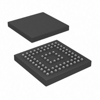
... OUTLINE DIMENSIONS * 1.40 MAX ORDERING GUIDE Max Speed Model (MHz) Digital 1 AD9393BBCZ- AD9393BBCZRL-80 80 AD9393/PCBZ RoHS Compliant Part. 6.10 6. 5.90 BALL A1 PAD CORNER 4.50 BSC SQ TOP VIEW 0.50 BSC BOTTOM VIEW 0.75 DETAIL A REF DETAIL A 0.15 MIN 0.35 0.30 0.25 BALL DIAMETER * COMPLIANT TO JEDEC STANDARDS MO-225 WITH THE EXCEPTION TO PACKAGE HEIGHT ...
Page 38
AD9393 NOTES Rev Page ...
Page 39
NOTES Rev Page AD9393 ...
Page 40
AD9393 NOTES ©2009 Analog Devices, Inc. All rights reserved. Trademarks and registered trademarks are the property of their respective owners. D08043-0-10/09(0) Rev Page ...