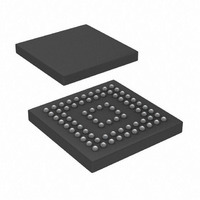
AD9393BBCZ-80 Analog Devices Inc, AD9393BBCZ-80 Datasheet - Page 7

AD9393BBCZ-80
Manufacturer Part Number
AD9393BBCZ-80
Description
Pb-free Low Power HDMI Rx
Manufacturer
Analog Devices Inc
Datasheet
1.AD9393BBCZ-80.pdf
(40 pages)
Specifications of AD9393BBCZ-80
Applications
Video
Interface
HDMI
Voltage - Supply
3.15 V ~ 3.47 V
Package / Case
76-CSPBGA
Mounting Type
Surface Mount
Lead Free Status / RoHS Status
Lead free / RoHS Compliant
Available stocks
Company
Part Number
Manufacturer
Quantity
Price
Company:
Part Number:
AD9393BBCZ-80
Manufacturer:
Analog Devices Inc
Quantity:
135
Company:
Part Number:
AD9393BBCZ-80
Manufacturer:
FUJ
Quantity:
1 445
Company:
Part Number:
AD9393BBCZ-80
Manufacturer:
Analog Devices Inc
Quantity:
10 000
Part Number:
AD9393BBCZ-80
Manufacturer:
ADI/亚德诺
Quantity:
20 000
Pin No.
References
Power Supply
Control
HDCP
Audio Data Outputs
Data Enable
RTERM
1
The supplies should be sequenced such that V
B8
A9
D10
E7, F7
D4, D5
F9, G9
G6, G7
C9, C10, D6, D7, D9, E4,
E9, E10,
A10
B10
H9
J9
F10
G10
J7
J6
J5
J4
J3
J2
G4
G5
B7
J8
F4, H10, J1, K3, K6, K9
1
Mnemonic
VSOUT
O/E
FILT
V
V
PV
DV
GND
SDA
SCL
DDC_SCL
DDC_SDA
MDA
MCL
S/PDIF
I2S0
I2S1
I2S2
I2S3
MCLK
SCLK
LRCLK
DE
RTERM
D
DD
DD
DD
D
and V
DD
Description
VSYNC Output Clock (Phase-Aligned with DCLK). Vertical Sync Output. The
separated VSYNC from a composite signal or a direct passthrough of the
VSYNC signal. The polarity of this output can be controlled via the serial bus
bit (Register 0x24[6]).
Odd/Even Field Output for Interlaced Video. This output identifies whether the
current field (in an interlaced signal) is odd or even. The polarity of this signal
is programmable via Register 0x24[4].
Connection for External Filter Components for Audio PLL. For proper operation,
the audio clock generator PLL requires an external filter. Connect the filter
shown in Figure 6 to this pin. For optimal performance, minimize noise and
parasitics on this node. For more information, see the PCB Layout
Recommendations section.
HDMI Terminator Power Supply
terminators. They should be as quiet and filtered as possible.
Digital Output Power Supply
to 27) switching at high speed (up to 80 MHz) generates many power supply
transients (noise). These supply pins are identified separately from the V
so output noise transferred into the sensitive circuitry can be minimized. If the
AD9393 is interfacing with lower voltage logic, V
lower supply voltage (as low as 1.8 V) for compatibility.
PLL Power Supply (1.8 V). The most sensitive portion of the AD9393 is the
clock generation circuitry. These pins provide power to the clock PLL and help
the user design for optimal performance. The user should provide quiet,
noise-free power to these pins.
Digital Logic Power Supply (1.8 V). These pins supply power to the digital
logic.
Ground. The ground return for all circuitry on chip. It is recommended that the
AD9393 be assembled on a single solid ground plane, with careful attention
to ground current paths.
Serial Port Data I/O for Programming the AD9393 Registers. The I
Address 0x98.
Serial Port Data Clock for Programming the AD9393 Registers.
HDCP Slave Serial Port Data Clock for HDCP Communications to Transmitter.
HDCP Slave Serial Port Data I/O for HDCP Communications to Transmitter. The
I
Master Serial Port I/O to EEPROM with HDCP Keys—I
Master Serial Port Data Clock to EEPROM with HDCP Keys.
S/PDIF Digital Audio Output.
I
I
I
I
Audio Master Clock Output for S/PDIF Data.
Audio Serial Clock Output for I
Data Output Clock for Left and Right Audio Channels.
Data Enable for Active Data Pixels.
Sets Internal Termination Resistance. Place a 500 Ω (1% tolerance) resistor from
this pin to ground. This sets the internal termination of TMDS lines to 50 Ω.
2
2
2
2
2
are never less than 300 mV below DV
C address is Address 0x74 or Address 0x76.
S Audio (Channel 1, Channel 2). Channel 0 and Channel 1 Audio Output.
S Audio (Channel 3, Channel 4). Channel 2 and Channel 3 Audio Output.
S Audio (Channel 5, Channel 6). Channel 4 and Channel 5 Audio Output.
S Audio (Channel 7, Channel 8). Channel 6 and Channel 7 Audio Output.
Rev. 0 | Page 7 of 40
(1.8 V
2
S Data.
DD
(3.3 V)
. At no time should DV
to
3.3 V)
. These pins supply power to the HDMI
. A large number of output pins (up
DD
can be connected to a
DD
2
C Address is 0xA0.
be more than 300 mV greater than V
2
C address is
D
pins,
AD9393
Value
V
V
PV
3.3 V
1.8 V to 3.3
V
1.8 V
1.8 V
0 V
3.3 V CMOS
3.3 V CMOS
3.3 V CMOS
3.3 V CMOS
3.3 V CMOS
3.3 V CMOS
V
V
V
V
V
V
V
V
3.3 V CMOS
500 Ω
DD
DD
DD
DD
DD
DD
DD
DD
DD
DD
DD
D
or V
DD
.


