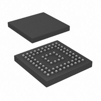
AD9393BBCZ-80 Analog Devices Inc, AD9393BBCZ-80 Datasheet - Page 12

AD9393BBCZ-80
Manufacturer Part Number
AD9393BBCZ-80
Description
Pb-free Low Power HDMI Rx
Manufacturer
Analog Devices Inc
Datasheet
1.AD9393BBCZ-80.pdf
(40 pages)
Specifications of AD9393BBCZ-80
Applications
Video
Interface
HDMI
Voltage - Supply
3.15 V ~ 3.47 V
Package / Case
76-CSPBGA
Mounting Type
Surface Mount
Lead Free Status / RoHS Status
Lead free / RoHS Compliant
Available stocks
Company
Part Number
Manufacturer
Quantity
Price
Company:
Part Number:
AD9393BBCZ-80
Manufacturer:
Analog Devices Inc
Quantity:
135
Company:
Part Number:
AD9393BBCZ-80
Manufacturer:
FUJ
Quantity:
1 445
Company:
Part Number:
AD9393BBCZ-80
Manufacturer:
Analog Devices Inc
Quantity:
10 000
Part Number:
AD9393BBCZ-80
Manufacturer:
ADI/亚德诺
Quantity:
20 000
AD9393
2-WIRE SERIAL REGISTER MAP
The AD9393 is initialized and controlled by a set of registers that determines the operating modes. An external controller is employed to
write and read the control registers through the 2-wire serial interface port.
Table 9. Control Register Map
Hex Address
0x00
0x01
0x02
0x03
0x11
0x12
0x17
0x18
0x22
0x23
0x24
0x25
Read/Write
Read
Read/write
Read/write
Read/write
Read/write
Read/write
Read
Read
Read/write
Read/write
Read/write
Read/write
Bits
[7:0]
[7:0]
[7:4]
[7:6]
[5:3]
[2]
[7:0]
[7]
[6]
[5]
[4]
[3:0]
[7:0]
[7:0]
[7:0]
[7]
[6]
[5]
[4]
[0]
[7:6]
[5:4]
[3:2]
[1]
[0]
Default
Value
00000000
01101001
1101xxxx
01xxxxxx
xx001xxx
xxxxx0xx
00000000
1xxxxxxx
x0xxxxxx
xx1xxxxx
xxx0xxxx
xxxx0000
00000000
4
32
1xxxxxxx
x1xxxxxx
xx1xxxxx
xxx1xxxx
xxxxxxx0
01xxxxxx
xx11xxxx
xxxx00xx
xxxxxx1x
xxxxxxx0
Register Name
Chip revision
PLL divider MSB
PLL divider LSB
VCO range
Charge pump
PLL enable
Reserved
Input HSYNC polarity
HSYNC polarity override
Input VSYNC polarity
VSYNC polarity override
HSYNCs per VSYNC MSB
HSYNCs per VSYNC LSB
VSYNC duration
HSYNC duration
HSYNC output polarity
VSYNC output polarity
DE output polarity
Field output polarity
Output CLK invert
Output CLK select
Output drive strength
Output mode
Primary output enable
Secondary output enable
Rev. 0 | Page 12 of 40
0 = active low.
Description
Chip revision ID. Revision is read [7:4] = major revision. [3:0]
= minor revision.
PLL feedback divider value MSB.
PLL feedback divider value LSB.
VCO range.
Charge pump current control for PLL.
This bit enables a lower frequency to be used for audio
MCLK generation.
Must be set to 0x00 (default).
0 = active low.
1 = active high.
0 = auto HSYNC polarity.
1 = manual HSYNC polarity.
1 = active high.
0 = auto VSYNC polarity.
1 = manual VSYNC polarity.
MSB of HSYNCs per VSYNC.
HSYNCs per VSYNC count.
VSYNC duration.
HSYNC duration. Sets the duration of the output HSYNC in
pixel clocks.
Output HSYNC polarity.
0 = active low output.
1 = active high output.
Output VSYNC polarity.
0 = active low output.
1 = active high output.
Output DE polarity.
0 = negative output.
1 = positive output.
Output field polarity.
0 = active low output.
1 = active high output.
0 = noninverted clock output.
1 = inverted clock output.
Selects which clock to use on output ball. 1× CLK is divided
down from TMDS clock input when pixel repetition is in use.
00 = ½× CLK.
01 = 1× CLK.
10 = 2× CLK.
11 = 90° phase 1× CLK.
Sets the drive strength of the outputs. 00 = lowest, 11 =
highest.
Selects the data output mapping.
00 = 4:4:4 mode (normal).
01 = 4:2:2 + DDR 4:2:2 on D[7:0].
10 = DDR 4:4:4 + DDR 4:2:2 on D[7:0].
11 = 12-bit 4:2:2.
Enables primary output.
Enables secondary output (DDR 4:2:2 in Output Mode 1
and Output Mode 2).


