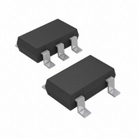
ADP1714AUJZ-1.8-R7 Analog Devices Inc, ADP1714AUJZ-1.8-R7 Datasheet - Page 11

ADP1714AUJZ-1.8-R7
Manufacturer Part Number
ADP1714AUJZ-1.8-R7
Description
300mA CMOS Low-Dropout Regular
Manufacturer
Analog Devices Inc
Datasheet
1.ADP1713-3.3-EVALZ.pdf
(16 pages)
Specifications of ADP1714AUJZ-1.8-R7
Regulator Topology
Positive Fixed
Voltage - Output
1.8V
Voltage - Input
2.5 ~ 5.5 V
Number Of Regulators
1
Current - Output
300mA (Max)
Current - Limit (min)
380mA
Operating Temperature
-40°C ~ 125°C
Mounting Type
Surface Mount
Package / Case
TSOT-23-5, TSOT-5, TSOP-5
Lead Free Status / RoHS Status
Lead free / RoHS Compliant
Voltage - Dropout (typical)
-
Lead Free Status / RoHS Status
Lead free / RoHS Compliant
Other names
ADP1714AUJZ-1.8-R7TR
Available stocks
Company
Part Number
Manufacturer
Quantity
Price
Company:
Part Number:
ADP1714AUJZ-1.8-R7
Manufacturer:
AD
Quantity:
60
ADJUSTABLE OUTPUT VOLTAGE
(ADP1712 ADJUSTABLE)
The ADP1712 adjustable version can have its output voltage
set over a 0.8 V to 5.0 V range. The output voltage is set by
connecting a resistive voltage divider from OUT to ADJ. The
output voltage is calculated using the equation
where:
R1 is the resistor from OUT to ADJ.
R2 is the resistor from ADJ to GND.
The maximum bias current into ADJ is 100 nA, so for less
than 0.5% error due to the bias current, use values less than
60 kΩ for R2.
BYPASS CAPACITOR (ADP1713)
The ADP1713 allows for an external bypass capacitor to be
connected to the internal reference, which reduces output
voltage noise and improves power supply rejection. A low
leakage capacitor of 1 nF or greater (10 nF is recommended)
must be connected between the BYP and GND pins.
TRACK MODE (ADP1714)
The ADP1714 includes a tracking mode feature. As shown in
Figure 28, if the voltage applied at the TRK pin is less than the
nominal output voltage, OUT is equal to the voltage at TRK.
Otherwise, OUT regulates to its nominal output value.
For example, consider an ADP1714 with a nominal output
voltage of 3 V. If the voltage applied to its TRK pin is greater than
3 V, OUT maintains a nominal output voltage of 3 V. If the volt-
age applied to TRK is reduced below 3 V, OUT tracks this voltage.
OUT can track the TRK pin voltage from the nominal value all
the way down to 0 V. A voltage divider is present from TRK to the
error amplifier input with a divider ratio equal to the divider
from OUT to the error amplifier. This sets the output voltage
equal to the tracking voltage. Both divider ratios are set by post-
package trim, depending on the desired output voltage.
V
OUT
Figure 28. ADP1714 Output Voltage vs. Tracking Voltage
4
3
2
1
0
= 0.8 V (1 + R1/R2)
0
with Nominal Output Voltage Set to 3 V
1
2
V
TRK
(V)
3
4
5
Rev. A | Page 11 of 16
(2)
ENABLE FEATURE
The ADP1712/ADP1713/ADP1714 use the EN pin to enable
and disable the OUT pin under normal operating conditions.
As shown in Figure 29, when a rising voltage on EN crosses the
active threshold, OUT turns on. When a falling voltage on EN
crosses the inactive threshold, OUT turns off.
As can be seen, the EN pin has hysteresis built in. This prevents
on/off oscillations that can occur due to noise on the EN pin as
it passes through the threshold points.
The EN pin active/inactive thresholds are derived from the IN
voltage. Therefore, these thresholds vary with changing input
voltage. Figure 30 shows typical EN active/inactive thresholds
when the input voltage varies from 2.5 V to 5.5 V.
UNDERVOLTAGE LOCKOUT (UVLO)
The ADP1712/ADP1713/ADP1714 have an undervoltage
lockout circuit, which monitors the voltage on the IN pin.
When the voltage on IN drops below 2 V (minimum), the
circuit activates, disabling the OUT pin.
1
1.4
1.3
1.2
1.1
1.0
0.9
0.8
0.7
0.6
0.5
Figure 29. ADP1712 Adjustable Typical EN Pin Operation
2.50
Figure 30. Typical EN Pin Thresholds vs. Input Voltage
2.75 3.00 3.25 3.50 3.75 4.00 4.25 4.50 4.75 5.00 5.25
ADP1712/ADP1713/ADP1714
OUT
EN
EN INACTIVE
EN ACTIVE
TIME (4ms/DIV)
V
IN
(V)
HYSTERESIS
V
V
C
I
LOAD
IN
OUT
OUT
= 5V
= 1.6V
= 2.2μF
= 10mA
5.50


