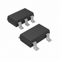
ADP1714AUJZ-1.8-R7 Analog Devices Inc, ADP1714AUJZ-1.8-R7 Datasheet - Page 4

ADP1714AUJZ-1.8-R7
Manufacturer Part Number
ADP1714AUJZ-1.8-R7
Description
300mA CMOS Low-Dropout Regular
Manufacturer
Analog Devices Inc
Datasheet
1.ADP1713-3.3-EVALZ.pdf
(16 pages)
Specifications of ADP1714AUJZ-1.8-R7
Regulator Topology
Positive Fixed
Voltage - Output
1.8V
Voltage - Input
2.5 ~ 5.5 V
Number Of Regulators
1
Current - Output
300mA (Max)
Current - Limit (min)
380mA
Operating Temperature
-40°C ~ 125°C
Mounting Type
Surface Mount
Package / Case
TSOT-23-5, TSOT-5, TSOP-5
Lead Free Status / RoHS Status
Lead free / RoHS Compliant
Voltage - Dropout (typical)
-
Lead Free Status / RoHS Status
Lead free / RoHS Compliant
Other names
ADP1714AUJZ-1.8-R7TR
Available stocks
Company
Part Number
Manufacturer
Quantity
Price
Company:
Part Number:
ADP1714AUJZ-1.8-R7
Manufacturer:
AD
Quantity:
60
ADP1712/ADP1713/ADP1714
Parameter
EN INPUT LOGIC HIGH
EN INPUT LOGIC LOW
EN INPUT LEAKAGE CURRENT
ADJ INPUT BIAS CURRENT
(ADP1712 ADJUSTABLE)
OUTPUT NOISE
POWER SUPPLY REJECTION RATIO
1
2
3
4
5
Accuracy when OUT is connected directly to ADJ. When OUT voltage is set by external feedback resistors, absolute accuracy in adjust mode depends on the tolerances
of resistors used.
Based on an end-point calculation using 10 mA and 300 mA loads. See
Dropout voltage is defined as the input-to-output voltage differential when the input voltage is set to the nominal output voltage. This applies only for output
voltages above 2.5 V.
Start-up time is defined as the time between the rising edge of EN to OUT being at 95% of its nominal value.
Current limit threshold is defined as the current at which the output voltage drops to 90% of the specified typical value. For example, the current limit for a 1.0 V
output voltage is defined as the current that causes the output voltage to drop to 90% of 1.0 V, or 0.9 V.
ADP1713
ADP1712 and ADP1714
ADP1713
ADP1712 and ADP1714
Symbol
V
V
V
ADJ
OUT
PSRR
IH
IL
I-LEAKAGE
I-BIAS
NOISE
Conditions
2.5 V ≤ V
2.5 V ≤ V
EN = IN or GND
10 Hz to 100 kHz, V
with 10 nF bypass capacitor
10 Hz to 100 kHz, V
1 kHz, V
bypass capacitor
1 kHz, V
Figure 10
IN
IN
Rev. A | Page 4 of 16
IN
IN
= 5.0 V, V
= 5.0 V, V
≤ 5.5 V
≤ 5.5 V
for typical load regulation performance for loads less than 10 mA.
OUT
OUT
IN
IN
= 5.0 V, V
= 5.0 V, V
= 0.75 V, with 10 nF
= 3.3 V
OUT
OUT
= 0.75 V,
= 3.3 V
Min
1.8
Typ
0.1
30
40
380
72
65
Max
0.4
1
100
Unit
V
V
μA
nA
μV rms
μV rms
dB
dB


