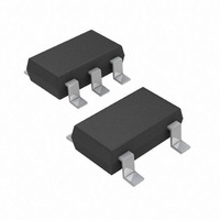
ADP1714AUJZ-1.8-R7 Analog Devices Inc, ADP1714AUJZ-1.8-R7 Datasheet - Page 6

ADP1714AUJZ-1.8-R7
Manufacturer Part Number
ADP1714AUJZ-1.8-R7
Description
300mA CMOS Low-Dropout Regular
Manufacturer
Analog Devices Inc
Datasheet
1.ADP1713-3.3-EVALZ.pdf
(16 pages)
Specifications of ADP1714AUJZ-1.8-R7
Regulator Topology
Positive Fixed
Voltage - Output
1.8V
Voltage - Input
2.5 ~ 5.5 V
Number Of Regulators
1
Current - Output
300mA (Max)
Current - Limit (min)
380mA
Operating Temperature
-40°C ~ 125°C
Mounting Type
Surface Mount
Package / Case
TSOT-23-5, TSOT-5, TSOP-5
Lead Free Status / RoHS Status
Lead free / RoHS Compliant
Voltage - Dropout (typical)
-
Lead Free Status / RoHS Status
Lead free / RoHS Compliant
Other names
ADP1714AUJZ-1.8-R7TR
Available stocks
Company
Part Number
Manufacturer
Quantity
Price
Company:
Part Number:
ADP1714AUJZ-1.8-R7
Manufacturer:
AD
Quantity:
60
ADP1712/ADP1713/ADP1714
PIN CONFIGURATIONS AND FUNCTION DESCRIPTIONS
Table 4. Pin Function Descriptions
ADP1712
Fixed
Pin No.
1
2
3
4
5
Figure 5. 5-Lead TSOT (UJ-Suffix)
GND
EN
IN
1
2
3
(Not to Scale)
ADP1712
TOP VIEW
FIXED
ADP1712
Adjustable
Pin No.
1
2
3
4
5
4
5
OUT
SS
ADP1713
Pin No.
1
2
3
4
5
Figure 6. 5-Lead TSOT (UJ-Suffix)
GND
EN
ADP1714
Pin No.
1
2
3
4
5
IN
1
2
3
ADJUSTABLE
(Not to Scale)
ADP1712
TOP VIEW
Mnemonic
IN
GND
EN
SS
ADJ
BYP
TRK
OUT
5
4
OUT
ADJ
Rev. A | Page 6 of 16
Description
Regulator Input Supply. Bypass IN to GND with a 2.2 μF or greater capacitor.
Ground.
Enable Input. Drive EN high to turn on the regulator; drive it low to turn
off the regulator. For automatic startup, connect EN to IN.
Soft Start. Connect a capacitor between SS and GND to set the output
start-up time.
Adjust. A resistor divider from OUT to ADJ sets the output voltage.
Bypass. Connect a 1 nF or greater capacitor (10 nF recommended)
between BYP and GND to reduce the internal reference noise for low
noise applications.
Track. The output follows the voltage placed on the TRK pin. (See the
Theory of Operation section for a more detailed description.)
Regulated Output Voltage. Bypass OUT to GND with a 2.2 μF or greater
capacitor.
Figure 7. 5-Lead TSOT (UJ-Suffix)
GND
EN
IN
1
2
3
(Not to Scale)
ADP1713
TOP VIEW
5
4
OUT
BYP
Figure 8. 5-Lead TSOT (UJ-Suffix)
GND
EN
IN
1
2
3
(Not to Scale)
ADP1714
TOP VIEW
5
4
OUT
TRK


