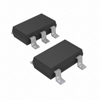
ADP1714AUJZ-1.8-R7 Analog Devices Inc, ADP1714AUJZ-1.8-R7 Datasheet - Page 14

ADP1714AUJZ-1.8-R7
Manufacturer Part Number
ADP1714AUJZ-1.8-R7
Description
300mA CMOS Low-Dropout Regular
Manufacturer
Analog Devices Inc
Datasheet
1.ADP1713-3.3-EVALZ.pdf
(16 pages)
Specifications of ADP1714AUJZ-1.8-R7
Regulator Topology
Positive Fixed
Voltage - Output
1.8V
Voltage - Input
2.5 ~ 5.5 V
Number Of Regulators
1
Current - Output
300mA (Max)
Current - Limit (min)
380mA
Operating Temperature
-40°C ~ 125°C
Mounting Type
Surface Mount
Package / Case
TSOT-23-5, TSOT-5, TSOP-5
Lead Free Status / RoHS Status
Lead free / RoHS Compliant
Voltage - Dropout (typical)
-
Lead Free Status / RoHS Status
Lead free / RoHS Compliant
Other names
ADP1714AUJZ-1.8-R7TR
Available stocks
Company
Part Number
Manufacturer
Quantity
Price
Company:
Part Number:
ADP1714AUJZ-1.8-R7
Manufacturer:
AD
Quantity:
60
ADP1712/ADP1713/ADP1714
140
120
100
140
120
100
140
120
100
80
60
40
20
80
60
40
20
80
60
40
20
0
0
0
0.5
0.5
0.5
MAX T
MAX T
MAX T
Figure 36. 500 mm
Figure 37. 100 mm
1.0
1.0
1.0
1mA
10mA
1mA
10mA
1mA
10mA
Figure 38. 0 mm
J
J
J
(DO NOT OPERATE ABOVE THIS POINT)
(DO NOT OPERATE ABOVE THIS POINT)
(DO NOT OPERATE ABOVE THIS POINT)
1.5
1.5
1.5
30mA
80mA
30mA
80mA
30mA
80mA
2.0
2.0
2.0
2
V
V
V
2
2
of PCB Copper, T
IN
IN
IN
2.5
2.5
2.5
of PCB Copper, T
of PCB Copper, T
– V
– V
– V
OUT
OUT
OUT
100mA
200mA
100mA
200mA
100mA
200mA
3.0
3.0
3.0
(V)
(V)
(V)
3.5
3.5
3.5
(LOAD CURRENT)
(LOAD CURRENT)
(LOAD CURRENT)
A
A
A
= 50°C
300mA
300mA
300mA
= 50°C
= 50°C
4.0
4.0
4.0
4.5
4.5
4.5
5.0
5.0
5.0
Rev. A | Page 14 of 16
PRINTED CIRCUIT BOARD LAYOUT
CONSIDERATIONS
Heat dissipation from the package can be improved by increasing
the amount of copper attached to the pins of the ADP1712/
ADP1713/ADP1714. However, as can be seen from Table 5, a
point of diminishing returns eventually is reached, beyond
which an increase in the copper size does not yield significant
heat dissipation benefits.
Place the input capacitor as close as possible to the IN and GND
pins. Place the output capacitor as close as possible to the OUT
and GND pins. For the ADP1712 adjustable version, place the
soft-start capacitor as close as possible to the SS pin. For the
ADP1713, place the internal reference bypass capacitor as close
as possible to the BYP pin. Use of 0402 or 0603 size capacitors
and resistors achieves the smallest possible footprint solution on
boards where area is limited.
GND (BOTTOM)
GND (TOP)
EN
IN
C1
Figure 39. Example PCB Layout
ADP1712/
ADP1713/
ADP1714
C3
SS/
ADJ/
BYP/
TRK
R1
C2
OUT
R2


