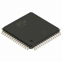
CY7C4255V-15ASXC Cypress Semiconductor Corp, CY7C4255V-15ASXC Datasheet - Page 14

CY7C4255V-15ASXC
Manufacturer Part Number
CY7C4255V-15ASXC
Description
CY7C4255V-15ASXC
Manufacturer
Cypress Semiconductor Corp
Series
CY7Cr
Datasheet
1.CY7C4255V-15ASXC.pdf
(24 pages)
Specifications of CY7C4255V-15ASXC
Function
Synchronous
Memory Size
144K (8K x 18)
Data Rate
100MHz
Access Time
10ns
Voltage - Supply
3.3V
Operating Temperature
-40°C ~ 85°C
Mounting Type
Surface Mount
Package / Case
64-LQFP
Lead Free Status / RoHS Status
Lead free / RoHS Compliant
Available stocks
Company
Part Number
Manufacturer
Quantity
Price
Company:
Part Number:
CY7C4255V-15ASXC
Manufacturer:
Cypress Semiconductor Corp
Quantity:
10 000
Switching Waveforms
Notes
Document Number: 38-06012 Rev. *D
19. The clocks (RCLK, WCLK) can be free-running during reset.
20. After reset, the outputs are LOW if OE = 0 and three-state if OE = 1.
21. When t
22. The first word is always available the cycle after EF goes HIGH.
t
CLK
Q
D
REN, WEN,
0
0
WCLK
RCLK
WEN
–D
–Q
+ t
REN
Q
EF,PAE
FF,PAF,
OE
SKEW2
EF
SKEW2
0 –
17
17
RS
Q
HF
LD
17
. The Latency Timing applies only at the Empty Boundary (EF = LOW).
> minimum specification, t
t
ENS
t
DS
Figure 9. First Data Word Latency after Reset with Simultaneous Read and Write
D
0
(FIRSTVALID WRITE)
(continued)
FRL
(maximum) = t
t
SKEW2
t
t
t
RSF
RSF
RSF
t
t
OLZ
RS
t
FRL
CLK
[21]
Figure 8. Reset Timing
+ t
SKEW2
t
D
REF
. When t
1
SKEW2
t
OE
< minimum specification, t
[19]
t
D
t
A
RSR
2
CY7C4255V, CY7C4265V
CY7C4275V, CY7C4285V
FRL
(maximum) = either 2 × t
D
0
t
A
[22]
D
3
OE=0
OE=1
CLK
[20]
+ t
Page 14 of 24
SKEW2
D
1
D
4
or
[+] Feedback


