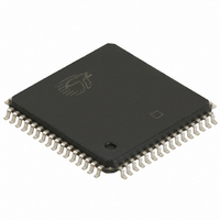
CY7C4255V-15ASXC Cypress Semiconductor Corp, CY7C4255V-15ASXC Datasheet - Page 7

CY7C4255V-15ASXC
Manufacturer Part Number
CY7C4255V-15ASXC
Description
CY7C4255V-15ASXC
Manufacturer
Cypress Semiconductor Corp
Series
CY7Cr
Datasheet
1.CY7C4255V-15ASXC.pdf
(24 pages)
Specifications of CY7C4255V-15ASXC
Function
Synchronous
Memory Size
144K (8K x 18)
Data Rate
100MHz
Access Time
10ns
Voltage - Supply
3.3V
Operating Temperature
-40°C ~ 85°C
Mounting Type
Surface Mount
Package / Case
64-LQFP
Lead Free Status / RoHS Status
Lead free / RoHS Compliant
Available stocks
Company
Part Number
Manufacturer
Quantity
Price
Company:
Part Number:
CY7C4255V-15ASXC
Manufacturer:
Cypress Semiconductor Corp
Quantity:
10 000
Programmable Almost Empty/Almost Full Flag
The CY7C4255/65/75/85V features programmable Almost
Empty and Almost Full Flags. Each flag can be programmed
(described in section
distance from the corresponding boundary flags (Empty or Full).
When the FIFO contains the number of words or fewer for which
Table 3. Flag Truth Table
Retransmit
The retransmit feature is beneficial when transferring packets of
data. It enables the receipt of data to be acknowledged by the
receiver and retransmitted if necessary.
The Retransmit (RT) input is active in the standalone and width
expansion modes. The retransmit feature is intended for use
when a number of writes equal to or less than the depth of the
FIFO have occurred and at least one word has been read since
the last RS cycle. A HIGH pulse on RT resets the internal read
pointer to the first physical location of the FIFO. WCLK and
RCLK may be free running but must be disabled during and t
after the retransmit pulse. With every valid read cycle after
retransmit, previously accessed data is read and the read pointer
is incremented until it is equal to the write pointer. Flags are
governed by the relative locations of the read and write pointers
and are updated during a retransmit cycle. Data written to the
FIFO after activation of RT are transmitted also. The full depth of
the FIFO can be repeatedly retransmitted.
Document Number: 38-06012 Rev. *D
0
1 to n
(n+1) to 4096
4097 to (8192–(m+1)) 8193 to (16384 –(m+1)) 16385 to (32768–(m+1)) 32769 to (65536 –(m+1))
(8192–m)
8192
Notes
2. n = Empty Offset (Default Values: CY7C4255/65/75/85V n = 127).
3. m = Full Offset (Default Values: CY7C4255/65/75/85V n = 127).
7C4255V – 8 K × 18
[2]
[3]
to 8192
Programming on page
0
1 to n
(n+1) to 8192
(16384–m)
16384
7C4265V – 16 K × 18
[2]
[3]
Number of Words in FIFO
to 16384
6) a specific
0
1 to n
(n+1) to 16384
(32768–m)
32768
7C4275V – 32 K × 18
[2]
RTR
[3]
to 32767
the flags have been programmed, the PAF or PAE is asserted,
signifying that the FIFO is either Almost Full or Almost Empty.
See
When the SMODE pin is tied LOW, the PAF flag signal transition
is caused by the rising edge of the write clock and the PAE flag
transition is caused by the rising edge of the read clock.
Width Expansion Configuration
The CY7C4255/65/75/85V can be expanded in width to provide
word widths greater than 18 in increments of 18. During width
expansion mode, all control line inputs are common and all flags
are available. Empty (Full) flags must be created by ANDing the
Empty (Full) flags of every FIFO. The PAE and PAF flags can be
detected from any one device. This technique avoids reading
data from, or writing data to the FIFO that is “staggered” by one
clock cycle due to the variations in skew between RCLK and
WCLK.
using two CY7C4255/65/75/85Vs.
Table 3
Figure 2 on page 8
0
1 to n
(n+1) to 32768
(65536–m)
65536
7C4285V – 64 K × 18
for a description of programmable flags.
[2]
[3]
to 65535
CY7C4255V, CY7C4265V
CY7C4275V, CY7C4285V
demonstrates a 36-word width by
FF PAF HF PAE EF
H
H
H
H
H
L
H
H
H
H
L
L
H
H
H
L
L
L
Page 7 of 24
H
H
H
H
L
L
H
H
H
H
H
L
[+] Feedback


