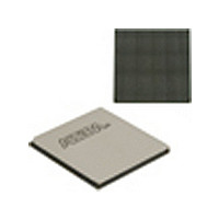
EP2SGX90EF1152I4 Altera, EP2SGX90EF1152I4 Datasheet - Page 13

EP2SGX90EF1152I4
Manufacturer Part Number
EP2SGX90EF1152I4
Description
Stratix II GX
Manufacturer
Altera
Datasheet
1.EP2SGX90EF1152I4.pdf
(316 pages)
Specifications of EP2SGX90EF1152I4
Family Name
Stratix II GX
Number Of Logic Blocks/elements
90960
# I/os (max)
558
Frequency (max)
732.1MHz
Process Technology
SRAM
Operating Supply Voltage (typ)
1.2V
Logic Cells
90960
Ram Bits
4520448
Operating Supply Voltage (min)
1.15V
Operating Supply Voltage (max)
1.25V
Operating Temp Range
-40C to 100C
Operating Temperature Classification
Industrial
Mounting
Surface Mount
Pin Count
1152
Package Type
FC-FBGA
Lead Free Status / Rohs Status
Not Compliant
Available stocks
Company
Part Number
Manufacturer
Quantity
Price
Company:
Part Number:
EP2SGX90EF1152I4
Manufacturer:
ALTERA
Quantity:
745
Company:
Part Number:
EP2SGX90EF1152I4N
Manufacturer:
ALTERA
Quantity:
535
Part Number:
EP2SGX90EF1152I4N
Manufacturer:
ALTERA/阿尔特拉
Quantity:
20 000
- Current page: 13 of 316
- Download datasheet (2Mb)
Figure 2–3. Clock Distribution for the Transmitters
Note to
(1)
Altera Corporation
October 2007
Reference Clocks
(refclks,
Global Clock (1) ,
Inter-Transceiver
Lines)
The global clock line must be driven by an input pin.
Figure
2–3:
Central Block
Transmitter Channel [3..2]
Transmitter Channel [1..0]
Transmitter PLL Block
The transmitter PLLs in each transceiver block clock the PMA and PCS
circuitry in the transmit path. The Quartus II software automatically
powers down the transmitter PLLs that are not used in the design.
Figure 2–4
The transmitter phase/frequency detector references the clock from one
of the following sources:
■
■
■
■
Two reference clocks, REFCLK0 and REFCLK1, are available per
transceiver block. The inter-transceiver block bus allows multiple
transceivers to use the same reference clocks. Each transceiver block has
one outgoing reference clock which connects to one inter-transceiver
block line. The incoming reference clock can be selected from five
inter-transceiver block lines IQ[4..0] or from the global clock line that
is driven by an input pin.
Reference clocks
Reference clock from the adjacent transceiver block
Inter-transceiver block clock lines
Global clock line driven by input pin
is a block diagram of the transmitter PLL.
Note (1)
Transmitter Local
Clock Divider Block
Transmitter Local
Clock Divider Block
Central Clock
Gen Block
Divider Block
Gen Block
TX Clock
TX Clock
Stratix II GX Device Handbook, Volume 1
Stratix II GX Architecture
Transmitter High-Speed &
Transmitter High-Speed &
Low-Speed Clocks
Low-Speed Clocks
2–5
Related parts for EP2SGX90EF1152I4
Image
Part Number
Description
Manufacturer
Datasheet
Request
R

Part Number:
Description:
CYCLONE II STARTER KIT EP2C20N
Manufacturer:
Altera
Datasheet:

Part Number:
Description:
CPLD, EP610 Family, ECMOS Process, 300 Gates, 16 Macro Cells, 16 Reg., 16 User I/Os, 5V Supply, 35 Speed Grade, 24DIP
Manufacturer:
Altera Corporation
Datasheet:

Part Number:
Description:
CPLD, EP610 Family, ECMOS Process, 300 Gates, 16 Macro Cells, 16 Reg., 16 User I/Os, 5V Supply, 15 Speed Grade, 24DIP
Manufacturer:
Altera Corporation
Datasheet:

Part Number:
Description:
Manufacturer:
Altera Corporation
Datasheet:

Part Number:
Description:
CPLD, EP610 Family, ECMOS Process, 300 Gates, 16 Macro Cells, 16 Reg., 16 User I/Os, 5V Supply, 30 Speed Grade, 24DIP
Manufacturer:
Altera Corporation
Datasheet:

Part Number:
Description:
High-performance, low-power erasable programmable logic devices with 8 macrocells, 10ns
Manufacturer:
Altera Corporation
Datasheet:

Part Number:
Description:
High-performance, low-power erasable programmable logic devices with 8 macrocells, 7ns
Manufacturer:
Altera Corporation
Datasheet:

Part Number:
Description:
Classic EPLD
Manufacturer:
Altera Corporation
Datasheet:

Part Number:
Description:
High-performance, low-power erasable programmable logic devices with 8 macrocells, 10ns
Manufacturer:
Altera Corporation
Datasheet:

Part Number:
Description:
Manufacturer:
Altera Corporation
Datasheet:

Part Number:
Description:
Manufacturer:
Altera Corporation
Datasheet:

Part Number:
Description:
Manufacturer:
Altera Corporation
Datasheet:

Part Number:
Description:
CPLD, EP610 Family, ECMOS Process, 300 Gates, 16 Macro Cells, 16 Reg., 16 User I/Os, 5V Supply, 25 Speed Grade, 24DIP
Manufacturer:
Altera Corporation
Datasheet:


