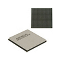
EP2SGX90EF1152I4 Altera, EP2SGX90EF1152I4 Datasheet - Page 297

EP2SGX90EF1152I4
Manufacturer Part Number
EP2SGX90EF1152I4
Description
Stratix II GX
Manufacturer
Altera
Datasheet
1.EP2SGX90EF1152I4.pdf
(316 pages)
Specifications of EP2SGX90EF1152I4
Family Name
Stratix II GX
Number Of Logic Blocks/elements
90960
# I/os (max)
558
Frequency (max)
732.1MHz
Process Technology
SRAM
Operating Supply Voltage (typ)
1.2V
Logic Cells
90960
Ram Bits
4520448
Operating Supply Voltage (min)
1.15V
Operating Supply Voltage (max)
1.25V
Operating Temp Range
-40C to 100C
Operating Temperature Classification
Industrial
Mounting
Surface Mount
Pin Count
1152
Package Type
FC-FBGA
Lead Free Status / Rohs Status
Not Compliant
Available stocks
Company
Part Number
Manufacturer
Quantity
Price
Company:
Part Number:
EP2SGX90EF1152I4
Manufacturer:
ALTERA
Quantity:
745
Company:
Part Number:
EP2SGX90EF1152I4N
Manufacturer:
ALTERA
Quantity:
535
Part Number:
EP2SGX90EF1152I4N
Manufacturer:
ALTERA/阿尔特拉
Quantity:
20 000
- Current page: 297 of 316
- Download datasheet (2Mb)
(1)
(2)
(3)
(4)
(5)
f
f
f
TCCS
SW
Output jitter
Output t
Output t
t
DPA run length
DPA jitter tolerance
DPA lock time
I N
H S D R
H S D R D PA
DUTY
Table 4–107. High-Speed I/O Specifications for -3 Speed Grade
= f
When J = 4 to 10, the SERDES block is used.
When J = 1 or 2, the SERDES block is bypassed.
For setup details, refer to the characterization report.
The input clock frequency and the W factor must satisfy the following fast PLL VCO specification: 150 ≤ input clock
frequency × W ≤ 1,040.
The minimum specification is dependent on the clock source (fast PLL, enhanced PLL, clock pin, and so on) and
the clock routing resource (global, regional, or local) utilized. The I/O differential buffer and input register do not
have a minimum toggle rate.
H S D R
(data rate)
R I S E
FA L L
Symbol
(DPA data rate) J = 4 to 10 (LVDS, HyperTransport technology)
/ W
(5)
W = 2 to 32 (LVDS, HyperTransport technology)
(3)
W = 1 (SERDES bypass, LVDS only)
W = 1 (SERDES used, LVDS only)
J = 4 to 10 (LVDS, HyperTransport technology)
J = 2 (LVDS, HyperTransport technology)
J = 1 (LVDS only)
All differential standards
All differential standards
All differential I/O standards
All differential I/O standards
Data channel peak-to-peak jitter
SPI-4
Parallel Rapid I/O
Miscellaneous
Table 4–107
grade Stratix II GX devices.
shows the high-speed I/O timing specifications for -3 speed
Conditions
0000000000
1111111111
00001111
10010000
10101010
01010101
100%
10%
25%
50%
Notes
0.44
Min
150
150
150
330
256
256
256
256
256
(1),
16
(4)
(4)
16
45
-3 Speed Grade
-
(2)
Typ
50
1,040
1,040
6,400
Max
520
500
717
760
500
200
190
160
180
55
-
Number of
repetitions
Mbps
Mbps
Mbps
Mbps
MHz
MHz
MHz
Unit
ps
ps
ps
ps
ps
UI
UI
%
Related parts for EP2SGX90EF1152I4
Image
Part Number
Description
Manufacturer
Datasheet
Request
R

Part Number:
Description:
CYCLONE II STARTER KIT EP2C20N
Manufacturer:
Altera
Datasheet:

Part Number:
Description:
CPLD, EP610 Family, ECMOS Process, 300 Gates, 16 Macro Cells, 16 Reg., 16 User I/Os, 5V Supply, 35 Speed Grade, 24DIP
Manufacturer:
Altera Corporation
Datasheet:

Part Number:
Description:
CPLD, EP610 Family, ECMOS Process, 300 Gates, 16 Macro Cells, 16 Reg., 16 User I/Os, 5V Supply, 15 Speed Grade, 24DIP
Manufacturer:
Altera Corporation
Datasheet:

Part Number:
Description:
Manufacturer:
Altera Corporation
Datasheet:

Part Number:
Description:
CPLD, EP610 Family, ECMOS Process, 300 Gates, 16 Macro Cells, 16 Reg., 16 User I/Os, 5V Supply, 30 Speed Grade, 24DIP
Manufacturer:
Altera Corporation
Datasheet:

Part Number:
Description:
High-performance, low-power erasable programmable logic devices with 8 macrocells, 10ns
Manufacturer:
Altera Corporation
Datasheet:

Part Number:
Description:
High-performance, low-power erasable programmable logic devices with 8 macrocells, 7ns
Manufacturer:
Altera Corporation
Datasheet:

Part Number:
Description:
Classic EPLD
Manufacturer:
Altera Corporation
Datasheet:

Part Number:
Description:
High-performance, low-power erasable programmable logic devices with 8 macrocells, 10ns
Manufacturer:
Altera Corporation
Datasheet:

Part Number:
Description:
Manufacturer:
Altera Corporation
Datasheet:

Part Number:
Description:
Manufacturer:
Altera Corporation
Datasheet:

Part Number:
Description:
Manufacturer:
Altera Corporation
Datasheet:

Part Number:
Description:
CPLD, EP610 Family, ECMOS Process, 300 Gates, 16 Macro Cells, 16 Reg., 16 User I/Os, 5V Supply, 25 Speed Grade, 24DIP
Manufacturer:
Altera Corporation
Datasheet:


