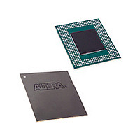
EPF10K50SBC356-2 Altera, EPF10K50SBC356-2 Datasheet - Page 50

EPF10K50SBC356-2
Manufacturer Part Number
EPF10K50SBC356-2
Description
FLEX 10KE
Manufacturer
Altera
Datasheet
1.EPF10K50SBC356-2.pdf
(100 pages)
Specifications of EPF10K50SBC356-2
Family Name
FLEX 10KE
Number Of Usable Gates
50000
Number Of Logic Blocks/elements
2880
# Registers
220
# I/os (max)
220
Frequency (max)
200MHz
Process Technology
CMOS
Operating Supply Voltage (typ)
2.5V
Logic Cells
2880
Ram Bits
40960
Device System Gates
199000
Operating Supply Voltage (min)
2.375V
Operating Supply Voltage (max)
2.625V
Operating Temp Range
0C to 85C
Operating Temperature Classification
Commercial
Mounting
Surface Mount
Pin Count
356
Package Type
BGA
Lead Free Status / Rohs Status
Not Compliant
Available stocks
Company
Part Number
Manufacturer
Quantity
Price
FLEX 10KE Embedded Programmable Logic Devices Data Sheet
Notes to tables:
(1)
(2)
(3)
(4)
(5)
(6)
(7)
(8)
(9)
(10) The I
(11) This value is specified for normal device operation. The value may vary during power-up.
(12) This parameter applies to -1 speed-grade commercial-temperature devices and -2 speed-grade-industrial
(13) Pin pull-up resistance values will be lower if the pin is driven higher than V
(14) Capacitance is sample-tested only.
50
Symbol
C
C
C
Table 23. FLEX 10KE Device Capacitance
IN
INCLK
OUT
See the
Minimum DC input voltage is –0.5 V. During transitions, the inputs may undershoot to –2.0 V for input currents
less than 100 mA and periods shorter than 20 ns.
Numbers in parentheses are for industrial-temperature-range devices.
Maximum V
All pins, including dedicated inputs, clock, I/O, and JTAG pins, may be driven before V
powered.
Typical values are for T
These values are specified under the FLEX 10KE Recommended Operating Conditions shown in
The FLEX 10KE input buffers are compatible with 2.5-V, 3.3-V (LVTTL and LVCMOS), and 5.0-V TTL and CMOS
signals. Additionally, the input buffers are 3.3-V PCI compliant when
in
The I
as well as output pins.
temperature devices.
Figure
OL
OH
Input capacitance
Input capacitance on
dedicated clock pin
Output capacitance
Operating Requirements for Altera Devices Data
parameter refers to low-level TTL, PCI, or CMOS output current. This parameter applies to open-drain pins
parameter refers to high-level TTL, PCI, or CMOS output current.
22.
CC
Parameter
rise time is 100 ms, and V
A
= 25 C, V
CCINT
V
V
V
IN
IN
OUT
CC
= 0 V, f = 1.0 MHz
= 0 V, f = 1.0 MHz
= 2.5 V, and V
= 0 V, f = 1.0 MHz
must rise monotonically.
Note (14)
Conditions
Sheet.
CCIO
= 2.5 V or 3.3 V.
V
CCIO
and V
CCIO
CCINT
Min
by an external source.
meet the relationship shown
CCINT
Max
Altera Corporation
10
12
10
and V
Tables 20
CCIO
Unit
are
pF
pF
pF
and 21.


