STGW35NB60S STMicroelectronics, STGW35NB60S Datasheet
STGW35NB60S
Specifications of STGW35NB60S
STGW35NB60S
Available stocks


Related parts for STGW35NB60S


STGW35NB60S Summary of contents
Page 1
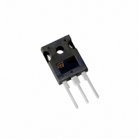
... MOTOR CONTROL STATIC RELAYS Order codes Sales Type STGW35NB60SD November 2005 N-CHANNEL 35A - 600V - TO-247 Low Drop PowerMESH™ IGBT I CE(sat) C @100°C < 1.7V 35A ) CEsat Internal schematic diagram outstanding Marking GW35NB60SD STGW35NB60SD TO-247 Package Packaging TO-247 TUBE Rev 1 1/13 www.st.com 13 ...
Page 2
... Purpose (1.6mm from case, for 10sec.) Table 2. Thermal resistance Rthj-case Thermal Resistance Junction-case (IGBT) Rthj-case Thermal Resistance Junction-case (DIODE) Rthj-amb Thermal Resistance Junction-ambient 2/13 Parameter = 25° 25°C C STGW35NB60SD Value 600 70 35 250 ± 200 – 150 300 Min. Typ. Max 0.625 ...
Page 3
... STGW35NB60SD 2 Electrical characteristics ( °C unless otherwise specified) CASE Table 3. Static Symbol Parameter Collectro-Emitter Breakdown V BR(CES) Voltage Collector-Emitter Saturation V CE(SAT) Voltage V Gate Threshold Voltage GE(th) Collector-Emitter Leakage I CES Current ( Gate-Emitter Leakage I GES Current ( Forward Transconductance fs Table 4. Dynamic Symbol Parameter C Input Capacitance ies ...
Page 4
... Tj=125° (see Figure 18) Test Conditions V = 480V 20A =100 , V = 15V, Tj= 25° (see Figure 18 480V 20A =100 , V = 15V, Tj= 125° (see Figure 18) STGW35NB60SD Min. Typ. Max. Unit 340 A/µ 320 A/µs 0.78 µs 1.1 µs 0.79 µs 1.1 µs 2.4 µs 1.2 µ ...
Page 5
... STGW35NB60SD Table 7. Collector-emitter diode Symbol Parameter V Forward On-Voltage Reverse Recovery Time Reverse Recovery Charge rr Reverse Recovery Current I rrm Softness factor of the diode Reverse Recovery Time Reverse Recovery Charge rr Reverse Recovery Current I rrm Softness factor of the diode S (1)Pulse width limited by max. junction temperature (2) Eon is the tun-on losses when a typical diode is used in the test circuit in figure 2 Eon include diode recovery energy. If the IGBT is offered in a package with a co-pak diode, the co-pack diode is used as external diode. IGBTs & ...
Page 6
... Electrical characteristics 2.1 Electrical characteristics (curves) Figure 1. Output Characteristics Figure 3. Transconductance Figure 5. Collector-Emitter on Voltage vs Collector Current 6/13 Figure 2. Transfer Characteristics Figure 4. Normalized Collector-Emitter On Voltage vs Temperature Figure 6. Gate Threshold vs Temperature STGW35NB60SD ...
Page 7
... STGW35NB60SD Figure 7. Normalized Breakdown Voltage vs Temperature Figure 9. Capacitance Variations Figure 11. Switching Losses vs Temperature 2 Electrical characteristics Figure 8. Gate Charge vs Gate-Emitter Voltage Figure 10. Switching Losses vs Gate Charge Figure 12. Switching Losses vs Collector Current 7/13 ...
Page 8
... Electrical characteristics Figure 13. Thermal Impedance Figure 15. Emitter-Collector Diode Characteristics 8/13 Figure 14. Turn-Off SOA STGW35NB60SD ...
Page 9
... STGW35NB60SD 3 Test Circuits Figure 16. Test Circuit for Inductive Load Switching Figure 18. Switching Waveform Figure 17. Gate Charge Test Circuit Figure 19. Diode Recovery Time Waveform 3 Test Circuits 9/13 ...
Page 10
... These packages have a Lead-free second level interconnect . The category of second level interconnect is marked on the package and on the inner box label, in compliance with JEDEC Standard JESD97. The maximum ratings related to soldering conditions are also marked on the inner box label. ECOPACK trademark. ECOPACK specifications are available at: www.st.com 10/13 STGW35NB60SD ...
Page 11
... STGW35NB60SD DIM. MIN. A 4.85 A1 2.20 b 1.0 b1 2.0 b2 3.0 c 0.40 D 19.85 E 15. 14.20 L1 3.70 L2 øP 3.55 øR 4.50 S TO-247 MECHANICAL DATA mm. TYP MAX. MIN. 5.15 0.19 2.60 0.086 1.40 0.039 2.40 0.079 3.40 0.118 0.80 0.015 20.15 0.781 15.75 0.608 5.45 14.80 ...
Page 12
... Revision History 5 Revision History Date Revision 16-Nov-2005 12/13 1 Initial release. STGW35NB60SD Changes ...
Page 13
... STGW35NB60SD Information furnished is believed to be accurate and reliable. However, STMicroelectronics assumes no responsibility for the consequences of use of such information nor for any infringement of patents or other rights of third parties which may result from its use. No license is granted by implication or otherwise under any patent or patent rights of STMicroelectronics. Specifications mentioned in this publication are subject to change without notice ...