STGD5NB120SZT4 STMicroelectronics, STGD5NB120SZT4 Datasheet
STGD5NB120SZT4
Specifications of STGD5NB120SZT4
Available stocks


Related parts for STGD5NB120SZT4


STGD5NB120SZT4 Summary of contents
Page 1
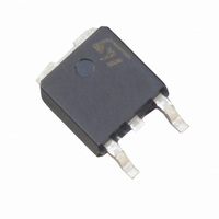
... Description This IGBT utilizes the advanced Power MESH™ process resulting in an excellent trade-off between switching performance and low on-state behavior. Table 1. Device summary Order codes STGD5NB120SZ-1 STGD5NB120SZT4 November 2008 1200 V - low drop internally clamped IGBT ) Figure 1. Marking GD5NB120SZ GD5NB120SZ Rev 7 ...
Page 2
Contents Contents 1 Electrical ratings . . . . . . . . . . . . . . . . . . . . . . . . . . . . . . . . . . . ...
Page 3
STGD5NB120SZ 1 Electrical ratings Table 2. Absolute maximum ratings Symbol V Collector-emitter voltage (V CES (1) Collector current (continuous (1) Collector current (continuous (2) Pulsed collector current I CP (3) Turn-off latching ...
Page 4
Electrical characteristics 2 Electrical characteristics (T =25 °C unless otherwise specified) CASE Table 4. Static electrical characteristics Symbol Collector-emitter breakdown voltage V (BR)CES ( Collector-emitter saturation V CE(sat) voltage V Gate threshold voltage GE(th) V Gate emitter ...
Page 5
STGD5NB120SZ Table 6. Switching on/off (inductive load) Symbol t Turn-on delay time d(on) t Current rise time r Turn-on current slope (di/dt Turn-on delay time d(on) t Current rise time r Turn-on current slope (di/dt Cross-over ...
Page 6
Electrical characteristics Electrical characteristics (curves) 2.1 Figure 2. Output characteristics Figure 4. Transconductance Figure 6. Gate charge vs gate-source voltage Figure 7. 6/15 Figure 3. Transfer characteristics Figure 5. Collector-emitter on voltage vs temperature Capacitance variations STGD5NB120SZ ...
Page 7
STGD5NB120SZ Figure 8. Normalized gate threshold voltage vs temperature Figure 10. Breakdown voltage vs temperature Figure 11. Normalized collector-emitter on Figure 12. Switching losses vs gate resistance Figure 13. Switching losses vs collector Electrical characteristics Figure 9. Collector-emitter on voltage ...
Page 8
Electrical characteristics Figure 14. Turn-off SOA 8/15 Figure 15. Thermal impedance K δ =0.5 0.2 0 0.05 0.02 0.01 single pulse - STGD5NB120SZ ZTH4 - ( ...
Page 9
STGD5NB120SZ 3 Test circuit Figure 16. Test circuit for inductive load switching Figure 18. Switching waveform Figure 17. Gate charge test circuit Test circuit 9/15 ...
Page 10
Package mechanical data 4 Package mechanical data In order to meet environmental requirements, ST offers these devices in ECOPACK® packages. These packages have a Lead-free second level interconnect. The category of second level interconnect is marked on the package and ...
Page 11
STGD5NB120SZ DIM TO-252 (DPAK) mechanical data mm. min. typ 2.20 0.90 0.03 0.64 5.20 0.45 0.48 6.00 5.10 6.40 4.70 ...
Page 12
Package mechanical data DIM (L1 12/15 TO-251 (IPAK) mechanical data mm. min. typ 2.20 0.90 0.64 5.20 0.45 0.48 6.00 6.40 2.28 4.40 16.10 9.00 ...
Page 13
STGD5NB120SZ 5 Packaging mechanical data DPAK FOOTPRINT All dimensions are in millimeters TAPE MECHANICAL DATA mm DIM. MIN. MAX 10.4 10.6 B1 12.1 D 1.5 1.6 D1 1.5 E 1.65 1.85 F 7.4 7.6 K0 2.55 ...
Page 14
Revision history 6 Revision history Table 9. Document revision history Date 06-Oct-2003 18-Jan-2005 13-Nov-2008 14/15 Revision 5 No history because migration 6 Final datasheet Table 2: Absolute maximum ratings 7 Insert new value in STGD5NB120SZ Changes ...
Page 15
... STGD5NB120SZ Information in this document is provided solely in connection with ST products. STMicroelectronics NV and its subsidiaries (“ST”) reserve the right to make changes, corrections, modifications or improvements, to this document, and the products and services described herein at any time, without notice. All ST products are sold pursuant to ST’s terms and conditions of sale. ...