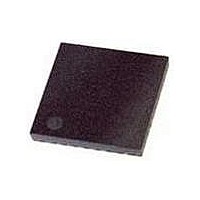
WM8973LGEFL/RV Wolfson Microelectronics, WM8973LGEFL/RV Datasheet - Page 18

WM8973LGEFL/RV
Manufacturer Part Number
WM8973LGEFL/RV
Description
Audio CODECs Stereo Codec with H/P Spkr
Manufacturer
Wolfson Microelectronics
Datasheet
1.WM8973LGEFLRV.pdf
(61 pages)
Specifications of WM8973LGEFL/RV
Maximum Operating Temperature
+ 85 C
Mounting Style
SMD/SMT
Package / Case
QFN-32
Minimum Operating Temperature
- 25 C
Lead Free Status / RoHS Status
Lead free / RoHS Compliant
Available stocks
Company
Part Number
Manufacturer
Quantity
Price
Part Number:
WM8973LGEFL/RV
Manufacturer:
WOLFSON
Quantity:
20 000
WM8973L
w
DEVICE DESCRIPTION
INTRODUCTION
INPUT SIGNAL PATH
The WM8973L is a low power audio codec offering a combination of high quality audio, advanced
features, low power and small size. These characteristics make it ideal for portable digital audio
applications such as MP3 and minidisk player / recorders. Stereo 24-bit multi-bit delta sigma ADCs
and DACs are used with oversampling digital interpolation and decimation filters.
The device includes three stereo analogue inputs that can be switched internally. Each can be used
as either a line level input or microphone input and LINPUT1/RINPUT1 and LINPUT2/RINPUT2 can
be configured as mono differential inputs. A programmable gain amplifier with automatic level control
(ALC) keeps the recording volume constant. The on-chip stereo ADC and DAC are of a high quality
using a multi-bit, low-order oversampling architecture to deliver optimum performance with low power
consumption.
The DAC output signal first enters an analogue mixer where an analogue input and/or the post-ALC
signal can be added to it. This mix is available on line and headphone outputs.
The WM8973L has a configurable digital audio interface where ADC data can be read and digital
audio playback data fed to the DAC. It supports a number of audio data formats including I
Mode (a burst mode in which frame sync plus 2 data packed words are transmitted), MSB-First, left
justified and MSB-First, right justified, and can operate in master or slave modes.
The WM8973L uses a unique clocking scheme that can generate many commonly used audio
sample rates from either a 12.00MHz USB clock or an industry standard 256/384 f
feature eliminates the common requirement for an external phase-locked loop (PLL) in applications
where the master clock is not an integer multiple of the sample rate. Sample rates of 8kHz,
11.025kHz, 12kHz, 16kHz, 22.05kHz, 24kHz, 32kHz, 44.1kHz, 48kHz, 88.2kHz and 96kHz can be
generated. The digital filters used for recording and playback are optimised for each sampling rate
used.
To allow full software control over all its features, the WM8973L offers a choice of 2 or 3 wire MPU
control interface. It is fully compatible and an ideal partner for a wide range of industry standard
microprocessors, controllers and DSPs.
The design of the WM8973L has given much attention to power consumption without compromising
performance. It operates at very low voltages, and includes the ability to power off parts of the
circuitry under software control, including standby and power off modes.
The input signal path for each channel consists of a switch to select between three analogue inputs,
followed by a PGA (programmable gain amplifier) and an optional microphone gain boost. A
differential input of either (LINPUT1 – RINPUT1) or (LINPUT2 – RINPUT2) may also be selected.
The gain of the PGA can be controlled either by the user or by the on-chip ALC function (see
Automatic Level Control).
The signal then enters an ADC where it is digitised. Alternatively, the two channels can also be
mixed in the analogue domain and digitised in one ADC while the other ADC is switched off. The
mono-mix signal appears on both digital output channels.
SIGNAL INPUTS
The WM8973L has three sets of high impedance, low capacitance AC coupled analogue inputs,
LINPUT1/RINPUT1, LINPUT2/RINPUT2 and LINPUT3/RINPUT3. Inputs can be configured as
microphone or line level by enabling or disabling the microphone gain boost.
LINSEL and RINSEL control bits (see Table 3) are used to select independently between external
inputs and internally generated differential products (LINPUT1-RINPUT1 or LINPUT2-RINPUT2). The
choice of differential signal, LINPUT1-RINPUT1 or LINPUT2-RINPUT2 is made using DS (refer to
Table 5).
As an example, the WM8973 can be set up to convert one differential and one single ended mono
signal by applying the differential signal to LINPUT1/RINPUT1 and the single ended signal to
RINPUT2. By setting LINSEL to L-R Differential (see Table 3), DS to LINPUT1 - RINPUT1 (see
Table 5) and RINSEL to RINPUT2, each mono signal can then be routed to a separate ADC or
Bypass path.
PD Rev 4.2 September 2005
Production Data
s
clock. This
2
S, DSP
18


