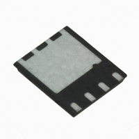
IRFH5210TR2PBF International Rectifier, IRFH5210TR2PBF Datasheet - Page 3

IRFH5210TR2PBF
Manufacturer Part Number
IRFH5210TR2PBF
Description
MOSFET N-CH 100V 55A 5X6 PQFN
Manufacturer
International Rectifier
Series
HEXFET®r
Type
Power MOSFETr
Datasheet
1.IRFH5210TR2PBF.pdf
(8 pages)
Specifications of IRFH5210TR2PBF
Fet Type
MOSFET N-Channel, Metal Oxide
Fet Feature
Logic Level Gate
Rds On (max) @ Id, Vgs
14.9 mOhm @ 33A, 10V
Drain To Source Voltage (vdss)
100V
Current - Continuous Drain (id) @ 25° C
10A
Vgs(th) (max) @ Id
4V @ 100µA
Gate Charge (qg) @ Vgs
59nC @ 10V
Input Capacitance (ciss) @ Vds
2570pF @ 25V
Power - Max
3.6W
Mounting Type
Surface Mount
Package / Case
8-PowerVQFN
Transistor Polarity
N-Channel
Drain-source Breakdown Voltage
100 V
Gate-source Breakdown Voltage
20 V
Continuous Drain Current
55 A
Power Dissipation
104 W
Gate Charge Qg
39 nC
Number Of Elements
1
Polarity
N
Channel Mode
Enhancement
Drain-source On-volt
100V
Gate-source Voltage (max)
±20V
Operating Temp Range
-55C to 150C
Operating Temperature Classification
Military
Mounting
Surface Mount
Pin Count
8
Lead Free Status / RoHS Status
Lead free / RoHS Compliant
Other names
IRFH5210TR2PBFTR
Available stocks
Company
Part Number
Manufacturer
Quantity
Price
Company:
Part Number:
IRFH5210TR2PBF
Manufacturer:
IOR
Quantity:
995
Part Number:
IRFH5210TR2PBF
Manufacturer:
IR
Quantity:
20 000
www.irf.com
Fig 5. Typical Capacitance vs.Drain-to-Source Voltage
100000
10000
1000
1000
0.01
100
1000
100
0.1
1.0
10
Fig 3. Typical Transfer Characteristics
100
10
Fig 1. Typical Output Characteristics
10
1
0.1
2
1
C rss
3.8V
T J = 150°C
C oss
C iss
V DS , Drain-to-Source Voltage (V)
V GS , Gate-to-Source Voltage (V)
V DS , Drain-to-Source Voltage (V)
3
V GS = 0V,
C iss = C gs + C gd , C ds SHORTED
C rss = C gd
C oss = C ds + C gd
1
4
V DS = 50V
≤60µs PULSE WIDTH
T J = 25°C
10
≤ 60µs PULSE WIDTH
Tj = 25°C
f = 1 MHZ
5
10
6
TOP
BOTTOM
100
7
VGS
15V
10V
7.0V
5.0V
4.5V
4.3V
4.0V
3.8V
1000
100
8
Fig 6. Typical Gate Charge vs.Gate-to-Source Voltage
Fig 4. Normalized On-Resistance vs. Temperature
1000
100
14.0
12.0
10.0
10
2.4
2.2
2.0
1.8
1.6
1.4
1.2
1.0
0.8
0.6
0.4
8.0
6.0
4.0
2.0
0.0
1
Fig 2. Typical Output Characteristics
0.1
-60 -40 -20 0 20 40 60 80 100 120 140 160
0
I D = 33A
V GS = 10V
I D = 33A
V DS , Drain-to-Source Voltage (V)
3.8V
T J , Junction Temperature (°C)
10
Q G , Total Gate Charge (nC)
1
20
V DS = 80V
V DS = 50V
VDS= 20V
≤ 60µs PULSE WIDTH
Tj = 150°C
10
30
TOP
BOTTOM
100
40
VGS
15V
10V
7.0V
5.0V
4.5V
4.3V
4.0V
3.8V
1000
50
3


