IRFIB6N60A Vishay, IRFIB6N60A Datasheet - Page 2
IRFIB6N60A
Manufacturer Part Number
IRFIB6N60A
Description
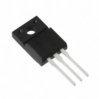
MOSFET N-CH 600V 5.5A TO220FP
Manufacturer
Vishay
Series
HEXFET®r
Datasheet
1.IRFIB6N60A.pdf
(8 pages)
Specifications of IRFIB6N60A
Fet Type
MOSFET N-Channel, Metal Oxide
Fet Feature
Standard
Rds On (max) @ Id, Vgs
750 mOhm @ 3.3A, 10V
Drain To Source Voltage (vdss)
600V
Current - Continuous Drain (id) @ 25° C
5.5A
Vgs(th) (max) @ Id
4V @ 250µA
Gate Charge (qg) @ Vgs
49nC @ 10V
Input Capacitance (ciss) @ Vds
1400pF @ 25V
Power - Max
60W
Mounting Type
Through Hole
Package / Case
TO-220-3 Full Pack (Straight Leads, Isolated), ITO-220AB
Configuration
Single
Transistor Polarity
N-Channel
Resistance Drain-source Rds (on)
0.75 Ohms
Drain-source Breakdown Voltage
600 V
Gate-source Breakdown Voltage
+/- 30 V
Continuous Drain Current
5.5 A
Power Dissipation
60 W
Maximum Operating Temperature
+ 150 C
Mounting Style
Through Hole
Minimum Operating Temperature
- 55 C
Lead Free Status / RoHS Status
Contains lead / RoHS non-compliant
Other names
*IRFIB6N60A
Available stocks
Company
Part Number
Manufacturer
Quantity
Price
Company:

Part Number:
IRFIB6N60A
Manufacturer:
IR
Quantity:
10 000
Company:
Part Number:
IRFIB6N60A
Manufacturer:
IR
Quantity:
12 500


Static @ T
Avalanche Characteristics
Thermal Resistance
Dynamic @ T
Diode Characteristics
R
R
E
I
E
I
V
R
V
I
I
I
V
t
Q
t
g
Q
Q
Q
t
t
t
t
C
C
C
C
C
C
DSS
AR
SM
GSS
S
rr
on
2
d(on)
r
d(off)
f
AS
AR
(BR)DSS
GS(th)
fs
SD
DS(on)
rr
g
gs
gd
iss
oss
rss
oss
oss
oss
JC
JA
eff.
Drain-to-Source Breakdown Voltage
Static Drain-to-Source On-Resistance
Gate Threshold Voltage
Gate-to-Source Forward Leakage
Gate-to-Source Reverse Leakage
Drain-to-Source Leakage Current
Continuous Source Current
(Body Diode)
Pulsed Source Current
(Body Diode)
Diode Forward Voltage
Reverse Recovery Time
Reverse RecoveryCharge
Forward Turn-On Time
Forward Transconductance
Total Gate Charge
Gate-to-Source Charge
Gate-to-Drain ("Miller") Charge
Turn-On Delay Time
Rise Time
Turn-Off Delay Time
Fall Time
Input Capacitance
Output Capacitance
Reverse Transfer Capacitance
Output Capacitance
Output Capacitance
Effective Output Capacitance
J
= 25°C (unless otherwise specified)
J
Junction-to-Case
Junction-to-Ambient
Single Pulse Avalanche Energy‚
Avalanche Current
Repetitive Avalanche Energy
= 25°C (unless otherwise specified)
Parameter
Parameter
Parameter
Parameter
Parameter
600
–––
–––
–––
–––
–––
–––
–––
Min. Typ. Max. Units
2.0
–––
–––
–––
–––
–––
–––
–––
–––
–––
–––
–––
Min. Typ. Max. Units
Min. Typ. Max. Units
5.5
–––
–––
–––
–––
–––
Intrinsic turn-on time is negligible (turn-on is dominated by L
1400 –––
1957 –––
–––
–––
–––
–––
–––
–––
–––
530
––– 0.75
––– -100
–––
–––
–––
–––
180
–––
3.0
7.1
13
25
30
22
49
96
–––
250
100
–––
–––
–––
–––
–––
–––
–––
–––
–––
800
4.0
1.5
4.4
5.5
25
49
13
20
37
µA
nA
µC
nC
ns
pF
ns
W
Typ.
V
V
V
S
Typ.
–––
–––
–––
–––
–––
V
V
V
V
V
V
V
MOSFET symbol
showing the
p-n junction diode.
T
V
V
V
V
I
R
R
V
ƒ = 1.0MHz, See Fig. 5
V
V
V
integral reverse
T
di/dt = 100A/µs „
V
I
D
D
J
J
GS
GS
DS
DS
DS
GS
GS
DS
DS
GS
DD
GS
DS
GS
GS
GS
G
D
= 9.2A
= 25°C, I
= 25°C, I
= 9.2A
= 35.5W,See Fig. 10
= 9.1W
= 600V, V
= 0V, I
= 10V, I
= V
= 480V, V
= 30V
= -30V
= 25V, I
= 400V
= 10V, See Fig. 6 and 13 „
= 300V
= 0V
= 25V
= 0V, V
= 0V, V
= 0V, V
GS
, I
D
S
F
D
DS
D
D
Conditions
DS
DS
= 250µA
Conditions
= 9.2A, V
= 9.2A
Conditions
= 250µA
= 3.3A
GS
GS
= 5.5A
Max.
= 0V to 480V …
Max.
= 1.0V, ƒ = 1.0MHz
= 480V, ƒ = 1.0MHz
290
2.1
9.2
6.0
65
= 0V
= 0V, T
www.irf.com
GS
„
J
G
= 0V
„
= 150°C
Units
Units
S
°C/W
+L
mJ
mJ
A
„
D
D
S
)
Related parts for IRFIB6N60A
Image
Part Number
Description
Manufacturer
Datasheet
Request
R

Part Number:
Description:
357-036-542-201 CARDEDGE 36POS DL .156 BLK LOPRO
Manufacturer:
Vishay
Datasheet:
Part Number:
Description:
357-036-542-201 CARDEDGE 36POS DL .156 BLK LOPRO
Manufacturer:
Vishay
Datasheet:
Part Number:
Description:
357-036-542-201 CARDEDGE 36POS DL .156 BLK LOPRO
Manufacturer:
Vishay
Datasheet:
Part Number:
Description:
357-036-542-201 CARDEDGE 36POS DL .156 BLK LOPRO
Manufacturer:
Vishay
Datasheet:
Part Number:
Description:
357-036-542-201 CARDEDGE 36POS DL .156 BLK LOPRO
Manufacturer:
Vishay
Datasheet:
Part Number:
Description:
357-036-542-201 CARDEDGE 36POS DL .156 BLK LOPRO
Manufacturer:
Vishay
Datasheet:
Part Number:
Description:
357-036-542-201 CARDEDGE 36POS DL .156 BLK LOPRO
Manufacturer:
Vishay
Datasheet:
Part Number:
Description:
357-036-542-201 CARDEDGE 36POS DL .156 BLK LOPRO
Manufacturer:
Vishay
Datasheet:
Part Number:
Description:
357-036-542-201 CARDEDGE 36POS DL .156 BLK LOPRO
Manufacturer:
Vishay
Datasheet:
Part Number:
Description:
357-036-542-201 CARDEDGE 36POS DL .156 BLK LOPRO
Manufacturer:
Vishay
Datasheet:
Part Number:
Description:
357-036-542-201 CARDEDGE 36POS DL .156 BLK LOPRO
Manufacturer:
Vishay
Datasheet:
Part Number:
Description:
357-036-542-201 CARDEDGE 36POS DL .156 BLK LOPRO
Manufacturer:
Vishay
Datasheet:
Part Number:
Description:
357-036-542-201 CARDEDGE 36POS DL .156 BLK LOPRO
Manufacturer:
Vishay
Datasheet:
Part Number:
Description:
357-036-542-201 CARDEDGE 36POS DL .156 BLK LOPRO
Manufacturer:
Vishay
Datasheet:
Part Number:
Description:
357-036-542-201 CARDEDGE 36POS DL .156 BLK LOPRO
Manufacturer:
Vishay
Datasheet: