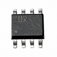
IRF7470PBF International Rectifier, IRF7470PBF Datasheet

IRF7470PBF
Specifications of IRF7470PBF
Available stocks
Related parts for IRF7470PBF
IRF7470PBF Summary of contents
Page 1
... Notes through „ are on page 8 www.irf.com SMPS MOSFET V DSS 40V Top View @ 10V GS @ 10V GS ƒ ƒ Typ. ––– ––– IRF7470PbF ® HEXFET Power MOSFET R max I DS(on) D 13mΩ 10A SO-8 Max. Units 40 V ± 12 ...
Page 2
... IRF7470PbF Static @ T = 25°C (unless otherwise specified) J Parameter V Drain-to-Source Breakdown Voltage (BR)DSS ∆V Breakdown Voltage Temp. Coefficient /∆T (BR)DSS J R Static Drain-to-Source On-Resistance DS(on) V Gate Threshold Voltage GS(th) I Drain-to-Source Leakage Current DSS Gate-to-Source Forward Leakage I GSS Gate-to-Source Reverse Leakage Dynamic @ T = 25°C (unless otherwise specified) ...
Page 3
... TOP BOTTOM 10 ° 1 0.1 100 Fig 2. Typical Output Characteristics 2 2.0 1.5 1.0 0.5 = 25V 0.0 2.8 3.0 -60 -40 -20 Fig 4. Normalized On-Resistance IRF7470PbF VGS 15V 10V 4.5V 3.0V 2.7V 2.5V 2.25V 2.0V 2.0V 20µs PULSE WIDTH ° 150 Drain-to-Source Voltage (V) DS 10A ...
Page 4
... IRF7470PbF 100000 0V MHZ C iss = rss = oss = 10000 Ciss 1000 Coss 100 Crss Drain-to-Source Voltage (V) Fig 5. Typical Capacitance Vs. Drain-to-Source Voltage 100 ° 150 ° 0.1 0.2 0.6 1.0 1.4 V ,Source-to-Drain Voltage (V) SD Fig 7. Typical Source-Drain Diode Forward Voltage 8.0A D SHORTED 100 Total Gate Charge (nC) Fig 6 ...
Page 5
... Fig 10. Maximum Effective Transient Thermal Impedance, Junction-to-Ambient www.irf.com Fig 10a. Switching Time Test Circuit V DS 90% 100 125 150 ° 10 Fig 10b. Switching Time Waveforms 0.001 0.01 0 Rectangular Pulse Duration (sec) 1 IRF7470PbF + - ≤ 1 ≤ 0 d(on) r d(off Notes: 1. Duty factor ...
Page 6
... IRF7470PbF 0.030 0.025 0.020 2.7V 0.015 4.5V 0.010 Drain Current (A) Fig 12. On-Resistance Vs. Drain Current Current Regulator Same Type as D.U. 50KΩ .2µF 12V .3µ D.U. 3mA Current Sampling Resistors Fig 13a&b. Basic Gate Charge Test Circuit and Waveform V (BR)DSS 20V Fig 14a&b. Unclamped Inductive Test circuit ...
Page 7
... L 7 6.46 [.255] 3X 1.27 [.050] DAT E CODE (YWW DES IGNAT ES LEAD-FREE PRODUCT (OPT IONAL LAS T DIGIT YEAR WW = WEEK XXXX EMBLY CODE F7101 LOT CODE PART NUMBER IRF7470PbF INCHE S MILLIMETERS DIM MIN MAX MIN MAX A .0532 .0688 1.35 1.75 A1 .0040 .0098 ...
Page 8
... IRF7470PbF SO-8 Tape and Reel Dimensions are shown in millimeters (inches) NOTES: 1. CONTROLLING DIMENSION : MILLIMETER. 2. ALL DIMENSIONS ARE SHOWN IN MILLIMETERS(INCHES). 3. OUTLINE CONFORMS TO EIA-481 & EIA-541. NOTES : 1. CONTROLLING DIMENSION : MILLIMETER. 2. OUTLINE CONFORMS TO EIA-481 & EIA-541. Notes: Repetitive rating; pulse width limited by max. junction temperature. ...


