STP5NK65ZFP STMicroelectronics, STP5NK65ZFP Datasheet
STP5NK65ZFP
Specifications of STP5NK65ZFP
Available stocks


Related parts for STP5NK65ZFP


STP5NK65ZFP Summary of contents
Page 1
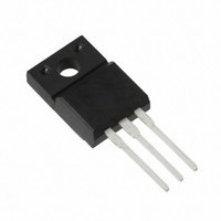
... Such series complements ST full range of high voltage Power MOSFETs including revolutionary MDmesh™ products Table 1. Device summary Order codes STP5NK65ZFP April 2009 N-channel 650 V, 1.5 Ω, 4.5 A TO-220FP 4 Figure 1. Marking Package P5NK65ZFP TO-220FP Doc ID 15565 Rev 1 STP5NK65ZFP TO-220FP Internal schematic diagram Packaging Tube www.st.com 1/12 12 ...
Page 2
... T Single pulse avalanche energy E AS (starting T 2/12 Parameter = ° 100 ° °C C =25 °C) C (BR)DSS. Parameter Parameter max ° Doc ID 15565 Rev 1 STP5NK65ZFP Value Unit 650 V ± (1) 4.5 A (1) 3 0.6 W/°C 2000 V 4.5 V/ns 2500 V -55 to 150 V Value Unit ...
Page 3
... STP5NK65ZFP 2 Electrical characteristics (Tcase =25 °C unless otherwise specified) Table 5. On/off states Symbol Drain-source V (BR)DSS breakdown voltage Zero gate voltage I DSS drain current (V Gate-body leakage I GSS current (V V Gate threshold voltage GS(th) Static drain-source on R DS(on) resistance Table 6. Dynamic Symbol (1) g Forward transconductance V ...
Page 4
... These integrated Zener diodes thus avoid the usage of external components. 4/12 Parameter Test conditions di/dt = 100 A/µ 100 Figure 20 Parameter Test conditions Igs=± 1mA (open drain) Doc ID 15565 Rev 1 STP5NK65ZFP Min. Typ 375 - 1.76 = 150 ° Min. Typ Max ...
Page 5
... STP5NK65ZFP 2.1 Electrical characteristics (curves) Figure 2. Safe operating area Tj=150°C 0.1 Tc=25°C Sinlge pulse 0.01 10 0.1 1 Figure 4. Output characteristics Figure 6. Transconductance Figure 3. AM03326v1 1µs 10µs 100µs 1ms 10ms V (V) 100 DS Figure 5. Figure 7. Doc ID 15565 Rev 1 Electrical characteristics ...
Page 6
... Gate charge vs gate-source voltage Figure 9. Figure 10. Normalized gate threshold voltage vs temperature Figure 12. Source-drain diode forward characteristics 6/12 Capacitance variations Figure 11. Normalized on resistance vs temperature Figure 13. Avalanche energy vs starting (mJ) 170 150 130 110 Doc ID 15565 Rev 1 STP5NK65ZFP AM03327v1 120 140 60 80 100 T (°C) J ...
Page 7
... STP5NK65ZFP Figure 14. Normalized BV DSS vs temperature Doc ID 15565 Rev 1 Electrical characteristics 7/12 ...
Page 8
... AM01468v1 Figure 18. Unclamped inductive load test 3.3 1000 µF µ AM01470v1 Figure 20. Switching time waveform V (BR)DSS 10% 0 AM01472v1 Doc ID 15565 Rev 1 STP5NK65ZFP 12V 47kΩ 100nF I =CONST G 100Ω GMAX 2200 µF 2.7kΩ 47kΩ 1kΩ circuit 2200 3.3 µ ...
Page 9
... STP5NK65ZFP 4 Package mechanical data In order to meet environmental requirements, ST offers these devices in different grades of ® ECOPACK packages, depending on their level of environmental compliance. ECOPACK specifications, grade definitions and product status are available at: www.st.com. ECOPACK trademark. Doc ID 15565 Rev 1 Package mechanical data ® 9/12 ...
Page 10
... Package mechanical data Dim 10/12 TO-220FP mechanical data Dia Doc ID 15565 Rev 1 STP5NK65ZFP 7012510_Rev_J ...
Page 11
... STP5NK65ZFP 5 Revision history Table 10. Document revision history Date 16-Apr-2009 Revision 1 First issue Doc ID 15565 Rev 1 Revision history Changes 11/12 ...
Page 12
... Australia - Belgium - Brazil - Canada - China - Czech Republic - Finland - France - Germany - Hong Kong - India - Israel - Italy - Japan - Malaysia - Malta - Morocco - Philippines - Singapore - Spain - Sweden - Switzerland - United Kingdom - United States of America 12/12 Please Read Carefully: © 2009 STMicroelectronics - All rights reserved STMicroelectronics group of companies www.st.com Doc ID 15565 Rev 1 STP5NK65ZFP ...