STP11NK50ZFP STMicroelectronics, STP11NK50ZFP Datasheet
STP11NK50ZFP
Specifications of STP11NK50ZFP
Available stocks


Related parts for STP11NK50ZFP


STP11NK50ZFP Summary of contents
Page 1
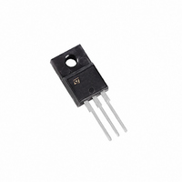
... PowerMESH™ layout. In addition to pushing on-resistance significantly down, special care is taken to ensure a very good dv/dt capability for the most demanding applications. Table 1. Device summary Order codes STB11NK50ZT4 STP11NK50ZFP STP11NK50Z May 2008 STB11NK50Z - STP11NK50ZFP TO-220 Figure 1. Marking Package B11NK50Z D²PAK P11NK50ZFP ...
Page 2
... Electrical characteristics (curves) 3 Test circuit 4 Package mechanical data . . . . . . . . . . . . . . . . . . . . . . . . . . . . . . . . . . . . 11 5 Packaging mechanical data 6 Revision history . . . . . . . . . . . . . . . . . . . . . . . . . . . . . . . . . . . . . . . . . . . 16 2/16 STB11NK50Z - STP11NK50ZFP - STP11NK50Z . . . . . . . . . . . . . . . . . . . . . . . . . . . . . . . . . . . . . . . . . . . . . . . ...
Page 3
... STB11NK50Z - STP11NK50ZFP - STP11NK50Z 1 Electrical ratings Table 2. Absolute maximum ratings Symbol V Drain-source voltage ( Gate-source voltage GS I Drain current (continuous Drain current (continuous (2) I Drain current (pulsed Total dissipation at T TOT Derating factor Gate source ESD (HBM-C= 100 pF, V ESD(G-S) R= 1.5 kΩ) (3) dv/dt ...
Page 4
... Total gate charge g Q Gate-source charge gs Gate-drain charge Pulsed: pulse duration=300µs, duty cycle 1. defined as a constant equivalent capacitance giving the same charging time as C oss eq. increases from 0 to 80% V 4/16 STB11NK50Z - STP11NK50ZFP - STP11NK50Z Parameter Test conditions mA Max rating Max rating @125 ° ± ...
Page 5
... STB11NK50Z - STP11NK50ZFP - STP11NK50Z Table 7. Switching times Symbol t Turn-on delay time d(on) t Rise time r t Turn-off delay time d(off) t Fall time f t Off-voltage rise time r(Voff) t Fall time f Cross-over time t c Table 8. Source drain diode Symbol I Source-drain current SD (1) Source-drain current (pulsed) ...
Page 6
... Electrical characteristics 2.1 Electrical characteristics (curves) Figure 2. Safe operating area for TO-220 / D²PAK Figure 4. Safe operating area for TO-220FP Figure 6. Output characteristics 6/16 STB11NK50Z - STP11NK50ZFP - STP11NK50Z Figure 3. Thermal impedance for TO-220 / D²PAK Figure 5. Thermal impedance for TO-220FP Figure 7. Transfer characteristics ...
Page 7
... STB11NK50Z - STP11NK50ZFP - STP11NK50Z Figure 8. Transconductance Figure 10. Gate charge vs gate-source voltage Figure 11. Capacitance variations Figure 12. Normalized gate threshold voltage vs temperature Electrical characteristics Figure 9. Static drain-source on resistance Figure 13. Normalized on resistance vs temperature 7/16 ...
Page 8
... Electrical characteristics Figure 14. Source-drain diode forward characteristics Figure 16. Maximum avalanche energy vs temperature 8/16 STB11NK50Z - STP11NK50ZFP - STP11NK50Z Figure 15. Normalized B VDSS vs temperature ...
Page 9
... STB11NK50Z - STP11NK50ZFP - STP11NK50Z 3 Test circuit Figure 17. Switching times test circuit for resistive load Figure 19. Test circuit for inductive load switching and diode recovery times Figure 21. Unclamped inductive waveform Figure 18. Gate charge test circuit Figure 20. Unclamped Inductive load test circuit Figure 22. Switching time waveform ...
Page 10
... These packages have a lead-free second level interconnect. The category of second level interconnect is marked on the package and on the inner box label, in compliance with JEDEC Standard JESD97. The maximum ratings related to soldering conditions are also marked on the inner box label. ECOPACK trademark. ECOPACK specifications are available at: 10/16 STB11NK50Z - STP11NK50ZFP - STP11NK50Z www.st.com ...
Page 11
... STB11NK50Z - STP11NK50ZFP - STP11NK50Z Dim L20 L30 ∅P Q TO-220 mechanical data mm Min Typ Max 4.40 4.60 0.61 0.88 1.14 1.70 0.48 0.70 15.25 15.75 1.27 10 10.40 2.40 2.70 4.95 5.15 1.23 1.32 6.20 6.60 2.40 2. 3.50 3.93 16.40 28.90 3.75 3.85 2.65 2 ...
Page 12
... Package mechanical data Dim Dia 12/16 STB11NK50Z - STP11NK50ZFP - STP11NK50Z TO-220FP mechanical data mm. Min. Typ Max. 4.40 4.60 2.5 2.7 2.5 2.75 0.45 0.70 0.75 1.00 1.15 1.50 1.15 1.50 4.95 5.20 2.40 2.70 10 10.40 16 28.6 30.6 9.80 10.60 2.9 3.6 15.90 16 ...
Page 13
... STB11NK50Z - STP11NK50ZFP - STP11NK50Z Dim D²PAK (TO-263) mechanical data mm Min Typ Max 4.40 4.60 0.03 0.23 0.70 0.93 1.14 1.70 0.45 0.60 1.23 1.36 8.95 9.35 7.50 10 10.40 8.50 2.54 4.88 5.28 15 15.85 2.49 2.69 2.29 2.79 1.27 1.40 1.30 1.75 0.4 0° ...
Page 14
... P2 1.9 2 0.25 0.35 0.0098 0.0137 W 23.7 24 sales type 14/16 STB11NK50Z - STP11NK50ZFP - STP11NK50Z TAPE AND REEL SHIPMENT inch MIN. MAX. 0.413 0.421 0.618 0.626 0.059 0.063 0.062 0.063 0.065 0.073 0.449 0.456 0.189 0.197 0.153 0.161 0.468 0.476 0.075 0.082 1 ...
Page 15
... STB11NK50Z - STP11NK50ZFP - STP11NK50Z 6 Revision history Table 10. Revision history Date 08-Sep-2005 14-Oct-2005 26-Mar-2006 29-Apr-2008 Revision 3 Complete version with curves 4 Inserted ecopack indication 5 New template, no content change 6 I value changed in GSS Revision history Changes Table 6 15/16 ...
Page 16
... Australia - Belgium - Brazil - Canada - China - Czech Republic - Finland - France - Germany - Hong Kong - India - Israel - Italy - Japan - Malaysia - Malta - Morocco - Singapore - Spain - Sweden - Switzerland - United Kingdom - United States of America 16/16 STB11NK50Z - STP11NK50ZFP - STP11NK50Z Please Read Carefully: © 2008 STMicroelectronics - All rights reserved STMicroelectronics group of companies www ...