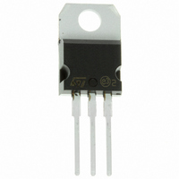
STP200NF03 STMicroelectronics, STP200NF03 Datasheet - Page 9

STP200NF03
Manufacturer Part Number
STP200NF03
Description
MOSFET N-CH 30V 120A TO-220
Manufacturer
STMicroelectronics
Series
STripFET™r
Datasheet
1.STB200NF03T4.pdf
(18 pages)
Specifications of STP200NF03
Fet Type
MOSFET N-Channel, Metal Oxide
Fet Feature
Standard
Rds On (max) @ Id, Vgs
3.6 mOhm @ 60A, 10V
Drain To Source Voltage (vdss)
30V
Current - Continuous Drain (id) @ 25° C
120A
Vgs(th) (max) @ Id
4V @ 250µA
Gate Charge (qg) @ Vgs
140nC @ 10V
Input Capacitance (ciss) @ Vds
4950pF @ 25V
Power - Max
300W
Mounting Type
Through Hole
Package / Case
TO-220-3 (Straight Leads)
Transistor Polarity
N Channel
Continuous Drain Current Id
60A
Drain Source Voltage Vds
30V
On Resistance Rds(on)
3.2mohm
Rds(on) Test Voltage Vgs
10V
Threshold Voltage Vgs Typ
4V
Rohs Compliant
Yes
Configuration
Single
Resistance Drain-source Rds (on)
0.0032 Ohms
Forward Transconductance Gfs (max / Min)
200 S
Drain-source Breakdown Voltage
30 V
Gate-source Breakdown Voltage
+/- 20 V
Continuous Drain Current
120 A
Power Dissipation
300 W
Maximum Operating Temperature
+ 175 C
Mounting Style
Through Hole
Minimum Operating Temperature
- 55 C
Lead Free Status / RoHS Status
Lead free / RoHS Compliant
Other names
497-6738-5
STP200NF03
STP200NF03
Available stocks
Company
Part Number
Manufacturer
Quantity
Price
Company:
Part Number:
STP200NF03
Manufacturer:
ST
Quantity:
12 500
Part Number:
STP200NF03
Manufacturer:
ST
Quantity:
20 000
STP200NF03 - STB200NF03 - STB200NF03-1
The previous curve gives the safe operating area for unclamped inductive loads, single
pulse or repetitive, under the following conditions:
P
E
Where:
I
P
t
To de rate above 25
I
Where:
Z
equal to T
AV
AV
AV
th
D(AVE)
AS(AR)
D(AVE)
is the Allowable Current in Avalanche
is the Time in Avalanche
= 2 * (T
= K * R
= 0.5 * (1.3 * BV
is the Average Power Dissipation in Avalanche (Single Pulse)
= P
AV
th
jmax
D(AVE)
.
is the value coming from Normalized Thermal Response at fixed pulse width
- T
CASE
* t
AV
o
C, at fixed I
)/ (1.3 * BV
DSS
* I
AV
AV
)
DSS
, the following equation must be applied:
* Z
th
)
Electrical characteristics
9/18


