STV240N75F3 STMicroelectronics, STV240N75F3 Datasheet
STV240N75F3
Specifications of STV240N75F3


Related parts for STV240N75F3


STV240N75F3 Summary of contents
Page 1
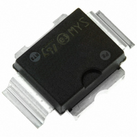
... N-channel 75 V, 2.3 mΩ, 240 A PowerSO-10 STripFET™ III Power MOSFET R DS(on max < 2.6 mΩ 240 A Figure 1. Marking 240N75F3 Doc ID 14595 Rev 2 STV240N75F3 10 1 PowerSO-10 Internal schematic diagram and connection diagram (top view) Package Packaging PowerSO-10 Tape and reel 1/15 www.st.com 15 ...
Page 2
... Contents Contents 1 Electrical ratings . . . . . . . . . . . . . . . . . . . . . . . . . . . . . . . . . . . . . . . . . . . . 3 2 Electrical characteristics . . . . . . . . . . . . . . . . . . . . . . . . . . . . . . . . . . . . . 4 2.1 Electrical characteristics (curves) 3 Test circuits 4 Package mechanical data . . . . . . . . . . . . . . . . . . . . . . . . . . . . . . . . . . . . 10 5 Packaging information . . . . . . . . . . . . . . . . . . . . . . . . . . . . . . . . . . . . . . 12 5.1 Tape and reel for PowerSO- Revision history . . . . . . . . . . . . . . . . . . . . . . . . . . . . . . . . . . . . . . . . . . . 14 2/ Doc ID 14595 Rev 2 STV240N75F3 ...
Page 3
... STV240N75F3 1 Electrical ratings Table 2. Absolute maximum ratings Symbol V Drain-source voltage ( Gate-source voltage GS I Drain current (continuous Drain current (continuous (1) Drain current (pulsed (2) Total dissipation TOT Derating factor (3) E Single pulse avalanche energy AS T Storage temperature stg T Operating junction temperature j 1. Pulse width limited by safe operating area 2 ...
Page 4
... Test conditions mA Max rating Max rating ± 250 µ 120 Parameter Test conditions MHz 37 (see Figure 14) Doc ID 14595 Rev 2 STV240N75F3 Min. Typ 125 ° 2.3 Min. Typ. 6800 =0 - 1100 120 Max. Unit V 10 µA 100 µA ±200 2.6 mΩ Max. Unit ...
Page 5
... STV240N75F3 Table 6. Switching times Symbol t Turn-on delay time d(on) t Rise time r t Turn-off delay time d(off) t Fall time f Table 7. Source drain diode Symbol I Source-drain current SD (1) I Source-drain current (pulsed) SD (2) V Forward on voltage SD t Reverse recovery time rr Q Reverse recovery charge rr I Reverse recovery current RRM 1 ...
Page 6
... V ( Figure 5. AM05545v1 ( temperature Figure 7. R DS(on) (mΩ) Doc ID 14595 Rev 2 STV240N75F3 Thermal impedance Zth_PowerSO-10 δ=0.5 0.2 0.1 0.05 0.02 0.01 Single pulse - Transfer characteristics Static drain-source on resistance 3.2 3.0 2.8 2.6 2.4 2.2 2.0 1.8 1 ...
Page 7
... STV240N75F3 Figure 8. Gate charge vs gate-source voltage Figure 9. Figure 10. Normalized gate threshold voltage vs temperature Figure 12. Source-drain diode forward characteristics Capacitance variations Figure 11. Normalized on resistance vs temperature Doc ID 14595 Rev 2 Electrical characteristics 7/15 ...
Page 8
... AM01468v1 Figure 16. Unclamped inductive load test 3.3 1000 µF µ AM01470v1 Figure 18. Switching time waveform V (BR)DSS 10% 0 AM01472v1 Doc ID 14595 Rev 2 STV240N75F3 12V 47kΩ 100nF I =CONST G 100Ω GMAX 2200 µF 2.7kΩ 47kΩ 1kΩ circuit 2200 3.3 µ ...
Page 9
... STV240N75F3 Figure 19. Gate charge test waveform Figure 20. Diode recovery times waveform SC15260 SC15250 Doc ID 14595 Rev 2 Test circuits 9/15 ...
Page 10
... Package mechanical data 4 Package mechanical data In order to meet environmental requirements, ST offers these devices in different grades of ® ECOPACK packages, depending on their level of environmental compliance. ECOPACK specifications, grade definitions and product status are available at: www.st.com. ECOPACK trademark. 10/15 Doc ID 14595 Rev 2 STV240N75F3 ® ...
Page 11
... STV240N75F3 DIM α PowerSO-10 MECHANICAL DATA mm MIN. TYP. MAX. 3.35 3.65 0.00 0.10 0.40 0.60 0.35 0.55 9.40 9.60 7.40 7.60 1.27 9.30 9.50 7.20 7.40 7.20 7.60 6.10 6.35 5.90 6.10 1.25 1.35 0.50 13.80 14.40 1.20 1.80 1. DETAIL "A" ...
Page 12
... Min. Typ. 14.9 15.0 9.9 10.0 4.15 4.25 11.4 11.5 1.65 1.75 23.7 24.0 1.9 2.0 3.9 4.0 23.9 24.0 0.025 0.30 1.50 1.55 (a) Doc ID 14595 Rev 2 STV240N75F3 Max. 15.1 10.1 4.35 11.6 1.85 24.3 2.1 4.1 24.1 0.35 1.60 ...
Page 13
... STV240N75F3 Table 9. Reel dimensions Ref Note: 10 sprocket hole pitch cumulative tolerance ±0.2 mm. Figure 22. Reel drawing Table 10. Base and bulk quantities a. Drawing is not to scale. b. Drawing is not to scale. Min. 1.5 12.8 20.2 60 (b) Base qty. 600 Doc ID 14595 Rev 2 Packaging information mm Typ. Max. ...
Page 14
... Revision history 6 Revision history Table 11. Document revision history Date 02-Apr-2008 21-Jan-2010 14/15 Revision 1 Initial release – Document status promoted from preliminary data to datasheet. 2 Section 5: Packaging – Inserted new Doc ID 14595 Rev 2 STV240N75F3 Changes information. ...
Page 15
... STV240N75F3 Information in this document is provided solely in connection with ST products. STMicroelectronics NV and its subsidiaries (“ST”) reserve the right to make changes, corrections, modifications or improvements, to this document, and the products and services described herein at any time, without notice. All ST products are sold pursuant to ST’s terms and conditions of sale. ...