STW45NM60 STMicroelectronics, STW45NM60 Datasheet
STW45NM60
Specifications of STW45NM60
Available stocks


Related parts for STW45NM60


STW45NM60 Summary of contents
Page 1
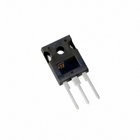
... Application ■ Switching application Order code Part number STW45NM60 April 2007 N-channel 650V@Tjmax - 0.09Ω - 45A - TO-247 R I DS(on) D < 0.11Ω 45A Internal schematic diagram Marking W45NM60 Rev 8 STW45NM60 MDmesh™ Power MOSFET TO-247 Package Packaging TO-247 Tube 1/12 www.st.com 12 ...
Page 2
... Contents Contents 1 Electrical ratings . . . . . . . . . . . . . . . . . . . . . . . . . . . . . . . . . . . . . . . . . . . . 3 2 Electrical characteristics . . . . . . . . . . . . . . . . . . . . . . . . . . . . . . . . . . . . . 4 2.1 Electrical characteristics (curves) 3 Test circuit 4 Package mechanical data . . . . . . . . . . . . . . . . . . . . . . . . . . . . . . . . . . . . . 9 5 Revision history . . . . . . . . . . . . . . . . . . . . . . . . . . . . . . . . . . . . . . . . . . . 11 2/ STW45NM60 . . . . . . . . . . . . . . . . . . . . . . . . . . . . . 6 ...
Page 3
... STW45NM60 1 Electrical ratings Table 1. Absolute maximum ratings Symbol V Gate- source voltage GS I Drain current (continuous Drain current (continuous (1) I Drain current (pulsed Total dissipation at T TOT Derating factor (2) dv/dt Peak diode recovery voltage slope T Storage temperature stg T Max. operating junction temperature j 1 ...
Page 4
... Parameter Test conditions V > D(on 22. 25V MHz 0V f=1 MHz Gate DC Bias = 0 test signal level = 20mV open drain V = 400V 10V GS Figure 14 DSS STW45NM60 Min. Typ. Max. Unit = 0 600 GS = 125 ° 250µ 22.5A 0.09 D Min. Typ. Max DS(on)max, 30 3800 = 0 1250 480V 340 DS 1 ...
Page 5
... STW45NM60 Table 6. Switching times Symbol t Turn-on delay time d(on) t Rise time r t Off-voltage rise time r(Voff) t Fall time f t Cross-over time c Table 7. Source drain diode Symbol I Source-drain current SD I Source-drain current (pulsed) SDM (1) V Forward on voltage SD t Reverse recovery time rr Q Reverse recovery charge ...
Page 6
... Electrical characteristics 2.1 Electrical characteristics (curves) Figure 1. Safe operating area Figure 3. Output characteristics Figure 5. Transconductance 6/12 Figure 2. Thermal impedance Figure 4. Transfer characteristics Figure 6. Static-drain source on resistance STW45NM60 ...
Page 7
... STW45NM60 Figure 7. Gate charge vs gate-source voltage Figure 8. Figure 9. Normalized gate threshold voltage vs temperature Figure 11. Source-drain diode forward characteristics Electrical characteristics Capacitance variations Figure 10. Normalized on resistance vs temperature Figure 12. Normalized BV DSS vs temperature 7/12 ...
Page 8
... Test circuit Figure 13. Switching times test circuit for resistive load Figure 15. Test circuit for inductive load switching and diode recovery times Figure 17. Unclamped inductive waveform 8/12 Figure 14. Gate charge test circuit Figure 16. Unclamped inductive load test circuit Figure 18. Switching time waveform STW45NM60 ...
Page 9
... STW45NM60 4 Package mechanical data In order to meet environmental requirements, ST offers these devices in ECOPACK® packages. These packages have a Lead-free second level interconnect. The category of second level interconnect is marked on the package and on the inner box label, in compliance with JEDEC Standard JESD97. The maximum ratings related to soldering conditions are also marked on the inner box label ...
Page 10
... STW45NM60 inch MIN. TYP. MAX. 0.19 0.20 0.086 0.102 0.039 0.055 0.079 0.094 0.118 0.134 0.015 0.03 0.781 0.793 0.608 0.620 ...
Page 11
... STW45NM60 5 Revision history Table 8. Revision history Date 05-Mar-2005 16-May-2006 18-Dec-2006 02-Apr-2007 Revision 5 Complete document with curves 6 The document has been reformatted 7 Updates curves:Figure 8 Figure 1. has been updated. Revision history Changes 1., Figure 4. and Figure 6. 11/12 ...
Page 12
... Australia - Belgium - Brazil - Canada - China - Czech Republic - Finland - France - Germany - Hong Kong - India - Israel - Italy - Japan - Malaysia - Malta - Morocco - Singapore - Spain - Sweden - Switzerland - United Kingdom - United States of America 12/12 Please Read Carefully: © 2007 STMicroelectronics - All rights reserved STMicroelectronics group of companies www.st.com STW45NM60 ...