NTB30N20T4G ON Semiconductor, NTB30N20T4G Datasheet - Page 2
NTB30N20T4G
Manufacturer Part Number
NTB30N20T4G
Description
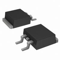
MOSFET N-CH 200V 30A D2PAK
Manufacturer
ON Semiconductor
Datasheet
1.NTB30N20T4G.pdf
(8 pages)
Specifications of NTB30N20T4G
Fet Type
MOSFET N-Channel, Metal Oxide
Fet Feature
Standard
Rds On (max) @ Id, Vgs
81 mOhm @ 15A, 10V
Drain To Source Voltage (vdss)
200V
Current - Continuous Drain (id) @ 25° C
30A
Vgs(th) (max) @ Id
4V @ 250µA
Gate Charge (qg) @ Vgs
100nC @ 10V
Input Capacitance (ciss) @ Vds
2335pF @ 25V
Power - Max
2W
Mounting Type
Surface Mount
Package / Case
D²Pak, TO-263 (2 leads + tab)
Configuration
Single
Transistor Polarity
N-Channel
Resistance Drain-source Rds (on)
0.081 Ohm @ 10 V
Forward Transconductance Gfs (max / Min)
20 S
Drain-source Breakdown Voltage
200 V
Gate-source Breakdown Voltage
+/- 30 V
Continuous Drain Current
30 A
Power Dissipation
214000 mW
Maximum Operating Temperature
+ 175 C
Mounting Style
SMD/SMT
Minimum Operating Temperature
- 55 C
Lead Free Status / RoHS Status
Lead free / RoHS Compliant
Other names
NTB30N20T4GOS
NTB30N20T4GOS
NTB30N20T4GOSTR
NTB30N20T4GOS
NTB30N20T4GOSTR
Available stocks
Company
Part Number
Manufacturer
Quantity
Price
Company:

Part Number:
NTB30N20T4G
Manufacturer:
ON
Quantity:
1 600
Company:
Part Number:
NTB30N20T4G
Manufacturer:
ON
Quantity:
12 500


3. Indicates Pulse Test: P. W. = 300 ms max, Duty Cycle = 2%.
4. Switching characteristics are independent of operating junction temperature.
ELECTRICAL CHARACTERISTICS
OFF CHARACTERISTICS
ON CHARACTERISTICS
DYNAMIC CHARACTERISTICS
SWITCHING CHARACTERISTICS (Notes 3 & 4)
BODY−DRAIN DIODE RATINGS (Note 3)
Drain−to−Source Breakdown Voltage
Temperature Coefficient (Positive)
Zero Gate Voltage Collector Current
Gate−Body Leakage Current (V
Gate Threshold Voltage
Temperature Coefficient (Negative)
Static Drain−to−Source On−State Resistance
Drain−to−Source On−Voltage
Forward Transconductance (V
Input Capacitance
Output Capacitance
Reverse Transfer Capacitance
Turn−On Delay Time
Rise Time
Turn−Off Delay Time
Fall Time
Gate Charge
Forward On−Voltage
Reverse Recovery Time
Reverse Recovery Stored Charge
(V
(V
(V
V
(V
(V
(V
(V
DS
GS
GS
GS
GS
GS
GS
GS
= V
= 0 Vdc, I
= 0 Vdc, V
= 0 Vdc, V
= 10 Vdc, I
= 10 Vdc, I
= 10 Vdc, I
= 10 Vdc, I
GS,
I
D
= 250 mAdc)
D
DS
DS
D
D
D
D
= 250 mAdc)
= 15 Adc)
= 10 Adc)
= 15 Adc, T
= 30 Adc)
= 200 Vdc, T
= 200 Vdc, T
DS
Characteristic
GS
J
= 15 Vdc, I
= 175°C)
J
J
= ± 30 Vdc, V
(V
(V
(V
(V
= 25°C)
= 175°C)
(I
DS
DS
DS
DS
S
(T
= 30 Adc, V
= 160 Vdc, V
= 25 Vdc, V
= 25 Vdc, V
= 25 Vdc, V
C
(V
(V
(V
(V
V
V
(I
(I
= 25°C unless otherwise noted)
DD
GS
DD
DS
DS
D
GS
S
S
= 30 Adc, V
= 15 Adc)
= 30 Adc, V
= 100 Vdc, I
= 160 Vdc, I
= 160 Vdc, I
= 160 Vdc, I
= 5.0 Vdc, R
dI
= 10 Vdc, R
DS
V
V
S
GS
/dt = 100 A/ms)
GS
= 0)
GS
GS
GS
GS
GS
= 5.0 Vdc)
= 10 Vdc)
= 0 Vdc, T
= 0 Vdc, f = 1.0 MHz)
= 0 Vdc, f = 1.0 MHz)
= 0 Vdc, f = 1.0 MHz)
http://onsemi.com
= 0 Vdc, f = 1.0 MHz)
GS
GS
D
D
D
D
G
NTB30N20
G
= 18 Adc,
= 30 Adc,
= 30 Adc,
= 18 Adc,
= 0 Vdc)
= 0 Vdc,
= 9.1 W)
= 2.5 W)
J
2
= 150°C)
V
Symbol
R
V
V
(BR)DSS
t
t
I
I
DS(on)
C
Q
DS(on)
C
V
GS(th)
g
C
d(on)
d(off)
Q
Q
Q
DSS
GSS
t
t
t
FS
oss
t
t
SD
iss
rss
RR
tot
gd
rr
a
b
r
gs
f
Min
200
2.0
−
−
−
−
−
−
−
−
−
−
−
−
−
−
−
−
−
−
−
−
−
−
−
−
−
−
−
−
−
−
−
−
−
0.068
0.067
0.200
2335
−8.9
0.91
0.80
1.85
Typ
307
380
148
230
140
2.9
2.0
20
75
10
12
20
70
40
82
24
88
75
48
20
16
32
85
−
−
−
−
0.081
0.080
0.240
± 100
Max
125
100
5.0
4.0
2.5
1.1
−
−
−
−
−
−
−
−
−
−
−
−
−
−
−
−
−
−
−
−
−
−
−
−
−
mV/°C
mV/°C
Mhos
mAdc
nAdc
Unit
Vdc
Vdc
Vdc
Vdc
pF
nC
mC
ns
ns
W
Related parts for NTB30N20T4G
Image
Part Number
Description
Manufacturer
Datasheet
Request
R

Part Number:
Description:
ON Semiconductor [VOLTAGE REGULATOR]
Manufacturer:
ON Semiconductor
Datasheet:
Part Number:
Description:
357-036-542-201 CARDEDGE 36POS DL .156 BLK LOPRO
Manufacturer:
ON Semiconductor
Datasheet:
Part Number:
Description:
357-036-542-201 CARDEDGE 36POS DL .156 BLK LOPRO
Manufacturer:
ON Semiconductor
Datasheet:
Part Number:
Description:
357-036-542-201 CARDEDGE 36POS DL .156 BLK LOPRO
Manufacturer:
ON Semiconductor
Datasheet:
Part Number:
Description:
357-036-542-201 CARDEDGE 36POS DL .156 BLK LOPRO
Manufacturer:
ON Semiconductor
Datasheet:
Part Number:
Description:
357-036-542-201 CARDEDGE 36POS DL .156 BLK LOPRO
Manufacturer:
ON Semiconductor
Datasheet:
Part Number:
Description:
357-036-542-201 CARDEDGE 36POS DL .156 BLK LOPRO
Manufacturer:
ON Semiconductor
Datasheet:
Part Number:
Description:
357-036-542-201 CARDEDGE 36POS DL .156 BLK LOPRO
Manufacturer:
ON Semiconductor
Datasheet:
Part Number:
Description:
357-036-542-201 CARDEDGE 36POS DL .156 BLK LOPRO
Manufacturer:
ON Semiconductor
Datasheet:
Part Number:
Description:
357-036-542-201 CARDEDGE 36POS DL .156 BLK LOPRO
Manufacturer:
ON Semiconductor
Datasheet:
Part Number:
Description:
357-036-542-201 CARDEDGE 36POS DL .156 BLK LOPRO
Manufacturer:
ON Semiconductor
Datasheet:
Part Number:
Description:
Manufacturer:
ON Semiconductor
Datasheet:
Part Number:
Description:
Manufacturer:
ON Semiconductor
Datasheet:
Part Number:
Description:
Manufacturer:
ON Semiconductor
Datasheet: